Top Manufacturers
Stock

Displaying 341 - 360 of 5453

Evaluation Kits from Analog Devices Inc.

LTC3614EUDD Demo Board | 4A, 4MHz Monolithic Synchronous Step-Down DC/DC Converter

Analog Devices Inc.
Demo Circuit 1467 is a high efficiency, high frequency step-down converter, incorporating the LTC3614 monolithic synchronous regulator. The DC1467A has an input voltage range of 2.25V to 5.5V, and is capable of delivering up to 4A of output current. The output voltage of the DC1467A can be set as low as 0.6V, the reference voltage of the LTC3614. The operating frequency range of the DC1467A is either set to a fixed 2.25 MHz by connecting the frequency pin to SVin, set by an external resistor, or synchronized to an external clock, with a range up to 4 MHz. At low load currents, the DC1467A can operate in either noise sensitive applications, due to the capability of the LTC3614 to operate in pulse-skipping mode, or in high efficiency applications, because the LTC3614 also has Burst-Mode capability. The Burst Mode clamp can be set externally.

DC2364A

Analog Devices Inc.
The LTC2873 is a robust pin-configurable multiprotocol transceiver that supports RS232, RS485, and RS422 protocols while operating on a single 3V to 5.5V supply. The LTC2873 can be configured as a half-duplex RS485 transceiver or as an RS232 transceiver using the same two bus pins.A pin-controlled integrated termination resistor allows for easy interface reconfiguration, eliminating external resistors and control relays. Loopback mode steers the driver inputs to the receiver outputs for diagnostic self-test. The RS485 receiver supports up to 256 nodes per bus, and features full failsafe operation for floating, shorted or terminated inputs.An integrated DC/DC boost converter uses a tiny 2mm ? 1.6mm inductor and one capacitor, eliminating the need for multiple supplies when driving RS232 levels.Applications Software Selectable RS232/RS485/RS422 Interface Industrial Sensors and Actuators Alarm Systems Traffic Control and Monitoring Highway Signs and Jumbo Displays

AD9516-2/PCBZ

Analog Devices Inc.
The AD9516-2?provides a multi-output clock distribution function with subpicosecond jitter performance, along with an on-chip PLL and VCO. The on-chip VCO tunes from 2.05 GHz to 2.33 GHz. Optionally, an external VCO/VCXO of up to 2.4 GHz can be used.The AD9516-2 emphasizes low jitter and phase noise to maximize data converter performance, and it can benefit other applications with demanding phase noise and jitter requirements. The AD9516-2 features six LVPECL outputs (in three pairs) and four LVDS outputs (in two pairs). Each LVDS output can be reconfigured as two CMOS outputs. The LVPECL outputs operate to 1.6 GHz, the LVDS outputs operate to 800 MHz, and the CMOS outputs operate to 250 MHz.Each pair of outputs has dividers that allow both the divide ratio and coarse delay (or phase) to be set. The range of division for the LVPECL outputs is 1 to 32. The LVDS/CMOS outputs allow a range of divisions up to a maximum of 1024.The AD9516-0 is available in a 64-lead LFCSP and can be operated from a single 3.3 V supply. An external VCO, which requires an extended voltage range, can be accommodated by connecting the charge pump supply (VCP) to 5 V. A separate LVPECL power supply can be from 2.5 V to 3.3 V (nominal).The AD9516-2 is specified for operation over the standard industrial range of ?40?C to +85?C.APPLICATIONS Low jitter, low phase noise clock distribution 10/40/100 Gb/sec networking line cards, including SONET, Synchronous Ethernet, OTU2/3/4 Forward error correction (G.710) Clocking high speed ADCs, DACs, DDSs, DDCs, DUCs, MxFEs High performance wireless transceivers ATE and high performance instrumentation

LTC4000EUFD-1 Demo Board I 20V ≤ VIN ≤ 60V, Battery Charger Controller and PowerPath Manager, MPPC, VOUT = 14.6V @ 5A

Analog Devices Inc.
Demonstration circuit 1830B is a battery charger controller and PowerPath™ manager with maximum power point control (MPPC) featuring the LTC4000-1. MPPC extracts near maximum power from high impedance sources such as solar panels, wind turbines or fuel cells. MPPC is achieved by means of an input voltage regulation control loop. This board should be connected to a front-end DC/DC power supply for a complete charger solution.

ADP2120-EVALZ

Analog Devices Inc.
The ADP2119?/ ADP2120 are low quiescent current, synchronous, step-down DC-to -DC regulators in a compact 3mm x3mm LFCSP_WD package. Both Devices use current mode, constant frequency pulse-width modulation (PWM) control scheme for excellent stability and transient response. Under light load condition, they can be configured to operate in pulse frequency modulation (PFM) mode that reduces switching frequency to save power.The ADP2119/ADP2120 can support input voltages from 2.3V to 5.5V. The output voltage can be adjusted from 0.6V to input voltage (VIN) for the adjustable version, while the fixed output version is available in preset output voltage options of 3.3V, 2.5V, 1.8V, 1.5V ,1.2V and 1.0V. The ADP2119/ADP2120 require minimal external parts and provide a high efficiency solution with their integrated power switches, synchronous rectifier, and internal compensation. Each IC draws less than 3 ?A current from the input source when it is disabled. Other key features include under voltage lockout(UVLO), integrated soft start to limit inrush current at startup, overvoltage protection (OVP), over current protection (OCP) and thermal shutdown (TSD).APPLICATIONS Point of load conversion Communications and networking equipment Industrial and instrumentation Consumer electronics Medical appliances

LTC3639EMSE Demo Board | Sync Buck, 4V ≤ VIN ≤ 150V, VOUT = 1.8V/3.3V/5V/Adj @ 100mA

Analog Devices Inc.
Demonstration circuit 1901A is a 150V input, 100mA output DC/DC power supply featuring the LTC3639. The IC operates in a high efficiency Burst Mode® operation and includes internal high and low side power MOSFETs. The board will accept an input voltage between 4V and 150V, and provide jumper selected output voltages of 1.8V, 3.3V, 5V and an option for additional voltages. The IC includes internal soft-start and a provision for increasing soft-start time.

DC2345A

Analog Devices Inc.
The LT8391 is a synchronous 4-switch buck-boost LED controller that regulates LED current from input voltage above, below, or equal to the output voltage. The proprietary peak-buck peak-boost current mode control scheme allows adjustable and synchronizable 150kHz to 650kHz fixed frequency operation, or internal ?15% triangle spread spectrum operation for low EMI. With 4V to 60V input, 0V to 60V output, and seamless low noise transitions between operation regions, the LT8391 is ideal for LED driver and battery charger applications in automotive, industrial, and battery-powered systems.The LT8391 provides both internal (up to 128:1) and external (up to 2000:1) LED current PWM dimming with a high-side PMOS switch. Two CTRL pins provide flexible 20:1 analog dimming with ?3% LED current accuracy at 100mV full scale. Fault protection is provided to detect an open or short LED condition, during which the LT8391 retries, latches off, or keeps running. Switching Frequency Max Output Power LT8391 Adjustable 150kHz - 650kHz 450W+ LT8391A 2MHz 50W+ APPLICATIONS Automotive Head Lamps/Running Lamps High Power LED Lighting

AD9516-4/PCBZ

Analog Devices Inc.
The AD9516-4?provides a multi-output clock distribution function with subpicosecond jitter performance, along with an on-chip PLL and VCO. The on-chip VCO tunes from 1.45 GHz to 1.80 GHz. Optionally, an external VCO/VCXO of up to 2.4 GHz can be used.The AD9516-4 emphasizes low jitter and phase noise to maximize data converter performance, and it can benefit other applications with demanding phase noise and jitter requirements.The AD9516-4 features six LVPECL outputs (in three pairs) and four LVDS outputs (in two pairs). Each LVDS output can be reconfigured as two CMOS outputs. The LVPECL outputs operate to 1.6 GHz, the LVDS outputs operate to 800 MHz, and the CMOS outputs operate to 250 MHz.Each pair of outputs has dividers that allow both the divide ratio and coarse delay (or phase) to be set. The range of division for the LVPECL outputs is 1 to 32. The LVDS/CMOS outputs allow a range of divisions, up to a maximum of 1024.The AD9516-4 is available in a 64-lead LFCSP and can be operated from a single 3.3 V supply. An external VCO, which requires an extended voltage range, can be accommodated by connecting the charge pump supply (VCP to 5 V. A separate LVPECL power supply can be from 2.5 V to 3.3 V (nominal).The AD9516-4 is specified for operation over the industrial range of ?40?C to +85?C.APPLICATIONS Low jitter, low phase noise clock distribution 10/40/100 Gb/sec networking line cards, including SONET, Synchronous Ethernet, OTU2/3/4 Forward error correction (G.710) Clocking high speed ADCs, DACs, DDSs, DDCs, DUCs, MxFEs High performance wireless transceivers ATE and high performance instrumentation?

DC1523A

Analog Devices Inc.
The LTC3789 is a high performance buck-boost switching regulator controller that operates from input voltages above, below or equal to the output voltage. The constant-frequency, current mode architecture allows a phase-lockable frequency of up to 600kHz, while an output current feedback loop provides support for battery charging. With a wide 4V to 38V (40V maximum) input and output range and seamless, low noise transitions between operating regions, the LTC3789 is ideal for automotive, telecom and battery-powered systems.The operating mode of the controller is determined through the MODE/PLLIN pin. The MODE/PLLIN pin can select between pulse-skipping mode and forced continuous mode operation and allows the IC to be synchronized to an external clock. Pulse-skipping mode offers high efficiency and low ripple at light loads, while forced continuous mode operates at a constant frequency for noise-sensitive applications.A PGOOD pin indicates when the output is within 10% of its designed set point. The LTC3789 is available in low profile 28-pin 4mm ? 5mm QFN and narrow SSOP packages.Applications Automotive Systems Distributed DC Power Systems High Power Battery-Operated Devices Industrial Control

LTC2971 Demo Board | High Voltage Two 2-Channel PMBus Power System Managers with Four Power Supply Rails

Analog Devices Inc.
The DC2875A is a demonstration system for the LTC2971 Power System Manager that interfaces to various regulators. The board contains all the circuitry needed to demonstrate a power system that utilizes two 2-channel LTC2971 devices that manage four power supplies. The four power supplies include various switching regulators for the purpose of demonstrating a variety of methods to sense voltage and current. The demo board provides a sophisticated 4-channel digitally programmable power supply system. The LTC2971 is a 2-channel I2C/SMBus/PMBus Power System Manager that features accurate input current and energy measurement and is capable of managing ±60V supplies. The device monitors input current and input voltage, and calculates input power and energy. The DC2875A demonstrates the ability of the LTC2971 to sequence, trim, margin, supervise, monitor, and log faults for four power supplies. The LTC2971 monitors each channel’s output voltage and output current and also monitors each channel’s external temperature sensor and its own internal die temperature. The DC2875A board contains four independent power supply rails. All four rails are based on DC/DC switching regulators. The +36V and +32V channels are managed by an LTC2971 and the ±24V channels are managed by an LTC2971-1. The board is pre-configured with these voltages and may be re-configured with feedback resistors. The LTpowerPlay® graphical user interface (GUI) supports this demonstration system and enables complete control of all the features of the LTC2971. Together, the LTpowerPlay software and DC2875A hardware system create a powerful development environment for designing and testing configuration settings of the LTC2971. LTpowerPlay stores these settings in the LTC2971 internal EEPROM or in a project file. The software displays all of the configuration settings and real time measurements from the Power System Management IC. Telemetry allows easy access and decoding of the fault log created by the LTC2971. The board comes preprogrammed with the EEPROM values appropriate for the four power supply rails on the DC2875A. Just plug and play! Order pre-programmed devices from Analog Devices Express (ADX) using LTpowerPlay.

LTC4418 Dual Channel Prioritized PowerPath Controller

Analog Devices Inc.
Demonstration circuit 2707B uses the LTC®4418 to arbitrate between two input supply rails, selecting the highest priority, valid supply to power the load. The V1 rail is defined to have higher priority and the V2 rail has lower priority. Both rails have individual overvoltage and undervoltage comparators for setting valid window thresholds with external resistive dividers. If the highest priority rail voltage V1 falls out of the defined window (overvoltage or undervoltage), the V2 rail, if it is valid, is enabled and powers the load. Two or more LTC4418s can be cascaded to provide switchover between more than two rails.

AD9546/PCBZ

Analog Devices Inc.
The AD9546 incorporates digitized clocking technology that efficiently transports and distributes clock signals in systems. Digitized clocking allows the design of flexible and scalable clock transport systems with well controlled phase (time) alignment. These characteristics make the AD9546 a leading choice for the design of network equipment that must meet the synchronization requirements for IEEE? 1588? boundary clocks per ITU-T G.8273.2 Class D. Digitized clocking is also relevant in applications requiring the accurate transport of frequency and phase to multiple usage endpoints (for example, distributing synchronized system reference (SYSREF) clocks to an array of ADC channels). The AD9546 supports existing and emerging International Telecommunications Union (ITU) standards for the delivery of frequency, phase, and time of day over service provider packet networks (ITU-T G.8262, ITU-T G.812, ITU-T G.813, ITU-T G.823, ITU-T G.824, ITU-T G.825, and ITU-T G.8273.2). The 10 clock outputs of the AD9546 synchronize to any one of up to eight input references. The digital phase-locked loops (DPLLs) reduce timing jitter associated with the external references, and the analog phase-locked loops (APLLs) provide frequency translation with low jitter output clocks. The digitally controlled loop and holdover circuitry continuously generate a low jitter output signal, even when all reference inputs fail. The AD9546 is available in a 48-lead LFCSP (7 mm ? 7 mm) package and operates over the ?40?C to +85?C temperature range. Throughout this data sheet, a single function of a multifunction pin name may be referenced when only that function is relevant (for example, M5 for SDO/M5). APPLICATIONS5G timing transport high precision synchronization Global positioning system (GPS), precision time protocol (PTP) (IEEE 1588), and synchronous Ethernet (SyncE) jitter cleanup and synchronization Optical transport networks (OTN), synchronous digital hierarchy (SDH), and macro and small cell base stations Small base station clocking (baseband and radio) Stratum 2, Stratum 3e, and Stratum 3 holdover, jitter cleanup, and phase transient control JESD204B support for analog-to-digital converter (ADC) and digital-to-analog converter (DAC) clocking Carrier Ethernet

EVAL-ADUM3166EBZ

Analog Devices Inc.
The ADuM3165/ADuM31661 are USB 2.0 port isolators, utilizing Analog Devices, Inc., iCoupler? technology to dynamically support all USB 2.0 data rates: low (1.5 Mbps), full (12 Mbps), or high (480 Mbps), as required. The devices support host isolation with automatic speed negotiation as well as peripheral isolation.High speed data is retimed for jitter reduction, requiring an external clock signal or crystal input. The ADuM3165 supports the clock or crystal input on the upstream side, and the ADuM3166 supports the clock or crystal input on the downstream side, offering two options to best suit the system design.The low power standby mode for downstream (Side 2) supports applications with limited available power, such as battery-operated peripherals. The upstream (Side 1) standby current meets USB 2.0 requirements for suspended operation.The isolators are specified over an extended industrial temperature range of ?55?C to +125?C and are available in a compact 20-lead shrink small outline package (SSOP) with 5.3 mm creepage and clearance.APPLICATIONS USB peripheral, USB host, and USB hub isolation Electronic test and measurement equipment Medical devices and integrated PCs Industrial PCs and isolated USB ports for debug or upgrade USB isolator modules and USB cable isolators1 Protected by U.S. Patents 5,952,849; 6,873,065; 6,903,578; and 7,075,329. Other patents are pending.

AD9910/PCBZ

Analog Devices Inc.
The AD9910 is a direct digital synthesizer (DDS) featuringan integrated 14-bit DAC and supporting sample rates up to1 GSPS. The AD9910 employs an advanced, proprietary DDStechnology that provides a significant reduction in power consumptionwithout sacrificing performance. The DDS/DACcombination forms a digitally programmable, high frequency,analog output synthesizer capable of generating a frequencyagile sinusoidal waveform at frequencies up to 400 MHz.The user has access to the three signal control parameters thatcontrol the DDS: frequency, phase, and amplitude. The DDSprovides fast frequency hopping and frequency tuning resolutionwith its 32-bit accumulator. With a 1 GSPS sample rate, thetuning resolution is ~0.23 Hz. The DDS also enables fast phaseand amplitude switching capability.The AD9910 is controlled by programming its internal controlregisters via a serial I/O port. The AD9910 includes an integratedstatic RAM to support various combinations of frequency, phase,and/or amplitude modulation. The AD9910 also supports a userdefined, digitally controlled, digital ramp mode of operation. Inthis mode, the frequency, phase, or amplitude can be variedlinearly over time. For more advanced modulation functions, ahigh speed parallel data input port is included to enable directfrequency, phase, amplitude, or polar modulation.The AD9910 is specified to operate over the extended industrialtemperature range.Applications Agile local oscillator (LO) frequency synthesis Programmable clock generators FM chirp source for radar and scanning systems Test and measurement equipment Acousto-optic device drivers Polar modulators Fast frequency hopping

AD9520-3/PCBZ

Analog Devices Inc.
The AD9520-31 provides a multioutput clock distribution function with subpicosecond jitter performance, along with an on-chip PLL and VCO. The on-chip VCO tunes from 1.72 GHz to 2.25 GHz. An external 3.3 V/5 V VCO/VCXO of up to 2.4 GHz can also be used.The AD9520 serial interface supports both SPI and I2C? ports. An in-package EEPROM can be programmed through the serial interface and store user-defined register settings for power-up and chip reset.The AD9520 features 12 LVPECL outputs in four groups. Any of the 1.6 GHz LVPECL outputs can be reconfigured as two 250 MHz CMOS outputs.Each group of outputs has a divider that allows both the divide ratio (from 1 to 32) and the phase (coarse delay) to be set.The AD9520 is available in a 64-lead LFCSP and can be operated from a single 3.3 V supply. The external VCO can have an operating voltage up to 5.5 V. A separate output driver power supply can be from 2.375 V to 3.465 V.The AD9520 is specified for operation over the standard industrial range of ?40?C to +85?C.1The AD9520 is used throughout this data sheet to refer to all the members of the AD9520 family. However, when AD9520-3 is used, it is referring to that specific member of the AD9520 family.Applications Low jitter, low phase noise clock distribution Clock generation and translation for SONET, 10Ge, 10G FC, and other 10 Gbps protocols Forward error correction (G.710) Clocking high speed ADCs, DACs, DDSs, DDCs, DUCs, MxFEs High performance wireless transceivers ATE and high performance instrumentation Broadband infrastructures

DC1936A

Analog Devices Inc.
The LTC3882 is a dual, PolyPhase DC/DC synchronous step-down switching regulator controller with PMBus compliant serial interface. It uses a constant frequency, leading-edge modulation, voltage mode architecture for excellent transient response and output regulation. Each PWM channel can produce output voltages from 0.5V to 5.25V using a wide range of 3.3V compatible power stages, including power blocks, DrMOS or discrete FET drivers. Up to four LTC3882s can operate in parallel for 2-, 3-, 4-, 6- or 8-phase operation.LTC3882 system configuration and monitoring is supported by the LTpowerPlay? software tool. The device?s serial interface can be used to read back input voltage, output voltage and current, temperature and fault status. A wide range of operating parameters can be set via the digital interface or stored in internal EEPROM for use at power up. Switching frequency and phase, output voltage and device address can also be programmed using external configuration resistors. PWM?Enable Output TG/BG Control HW?Write Protect Dedicated PGOOD Differential Vout Sense LTC3882 Yes Yes Yes No? VOUT0 Only LTC3882-1 ?No No No Yes VOUT0 & VOUT1 Applications High Current Distributed Power Systems Servers, Network and Storage Equipment Intelligent Energy Efficient Power Regulation Industrial/Telecom/ATE Systems

AD9516-5/PCBZ

Analog Devices Inc.
The AD9516-5?provides a multi-output clock distribution function with subpicosecond jitter performance, along with an on-chip PLL that can be used with an external VCO/VCXO of up to 2.4 GHz.The AD9516-5 emphasizes low jitter and phase noise to maximize data converter performance, and it can benefit otherapplications with demanding phase noise and jitter requirements.The AD9516-5 features six LVPECL outputs (in three pairs)and four LVDS outputs (in two pairs). Each LVDS output canbe reconfigured as two CMOS outputs. The LVPECL outputsoperate to 1.6 GHz, the LVDS outputs operate to 800 MHz, andthe CMOS outputs operate to 250 MHz.Each pair of outputs has dividers that allow both the divide ratio and coarse delay (or phase) to be set. The range of division forthe LVPECL outputs is 1 to 32. The LVDS/CMOS outputs allowa range of divisions up to a maximum of 1024.The AD9516-5 is available in a 64-lead LFCSP and can beoperated from a single 3.3 V supply. An external VCO, which requires an extended voltage range, can be accommodated by connecting the charge pump supply (VCP) to 5.5 V. A separate LVPECL power supply can be from 2.375 V to 3.6 V (nominal).The AD9516-5 is specified for operation over the industrial range of ?40?C to +85?C.For applications requiring an integrated EEPROM, or needing additional outputs, the AD9520-5?and AD9522-5?are available.APPLICATIONS Low jitter, low phase noise clock distribution 10/40/100 Gb/sec networking line cards, including SONET, Synchronous Ethernet, OTU2/3/4 Forward error correction (G.710) Clocking high speed ADCs, DACs, DDSs, DDCs, DUCs, MxFEs High performance wireless transceivers ATE and high performance instrumentation

DC468A

Analog Devices Inc.
The LT5506 is a 40MHz to 500MHz monolithic integrated quadrature demodulator with variable gain amplifier (VGA), designed for low voltage operation. It supports standards that use a linear modulation format. The chip consists of a VGA, quadrature down-converting mixers and lowpass noise filters. The LO port consists of a divide-by-two stage and LO buffers. The IC provides all building blocks for IF down-conversion to I and Q baseband signals with a single supply voltage of 1.8V to 5.25V. The VGA gain has a linear-in- dB relationship to the control input voltage. Hard-clipping amplifiers at the mixer outputs reduce the recovery time from a signal overload condition. The lowpass filters reduce the out-of-band noise and spurious frequency components. The cut-off frequency of the noise filters is approximately 8.8MHz. The external 2xLO frequency is required to be twice the IF input frequency for the mixers. The standby mode provides reduced supply current and fast transient response into the normal operating mode when the I/Q outputs are AC-coupled to a baseband chip.Applications IEEE802.11 High Speed Wireless LAN Wireless Local Loop

LTC3610EUP Demo Board | Monolithic, 4.5V ≤ VIN ≤ 24V, VOUT = 1.2V/1.5V/1.8V/2.5V @ 12A

Analog Devices Inc.
Demonstration circuit DC1129A is a synchronous step down converter featuring the LTC3610, the high efficiency, high density DC/DC regulator. The input voltage range is from 4.5V to 24V. The output voltage is jumper-selectable and provides 1.2V, 1.5V, 1.8V or 2.5V at 12A load current. The regulator includes the controller and power MOSFETs in the 9mm by 9 mm QFN package.

ADRV9008-2W/PCBZ

Analog Devices Inc.
The ADRV9008-2 is a highly integrated, RF agile transmit subsystem offering dual channel transmitters, observation path receiver, integrated synthesizers, and digital signal processing functions. The IC delivers a versatile combination of high performance and low power consumption demanded by 2G, 3G and 4G macro-cell base stations, and active antenna, applications.The transmitters use an innovative direct conversion modulator that achieves multi-carrier macro-base-station quality performance and very low power. In 3G/4G mode, the maximum large-signal bandwidth is 200MHz. In MC-GSM mode, which has higher in-band SFDR, the maximum large-signal bandwidth is 75MHz.The observation path consists of a wide bandwidth direct-conversion receiver with state-of-the-art dynamic range. The complete receive subsystem includes dc offset correction, quadrature correction, and digital filtering thus eliminating the need for these functions in the digital baseband. Several auxiliary functions such as ADCs, DACs, and GPIOs for PA and RF-front-end control are also integrated. The fully integrated phase locked loops (PLLs) provide high performance, low power fractional-N RF frequency synthesis for the transmitter and receiver sections. An additional synthesizer is used to generate the clocks needed for the converters, digital circuits, and the serial interface. Special precautions have been taken to provide the isolation demanded in high performance base station applications. All VCO and loop filter components are integrated.The high-speed JESD204B interface supports up to 12.288 Gbps lane rates resulting in two lanes per transmitter in the widest bandwidth mode and two lanes for the observation path receiver in the widest bandwidth mode. The core of the ADRV9008-2 can be powered directly from 1.3 V and 1.8 V regulators and is controlled via a standard 4 wire serial port. Comprehensive power-down modes are included to minimize power consumption in normal use. The ADRV9008-2 is packaged in a 12mm ? 12 mm, 196-ball chip scale ball grid array (CSP_BGA).

Displaying 341 - 360 of 5453

Latest Parts

IN STOCK 13664
Buy

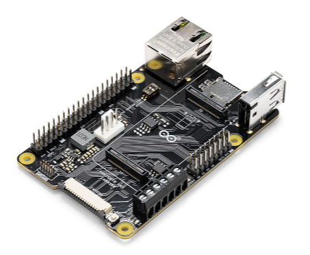
ASX00049

Arduino

* $43.18 - * $50.33

IN STOCK 2847
Buy

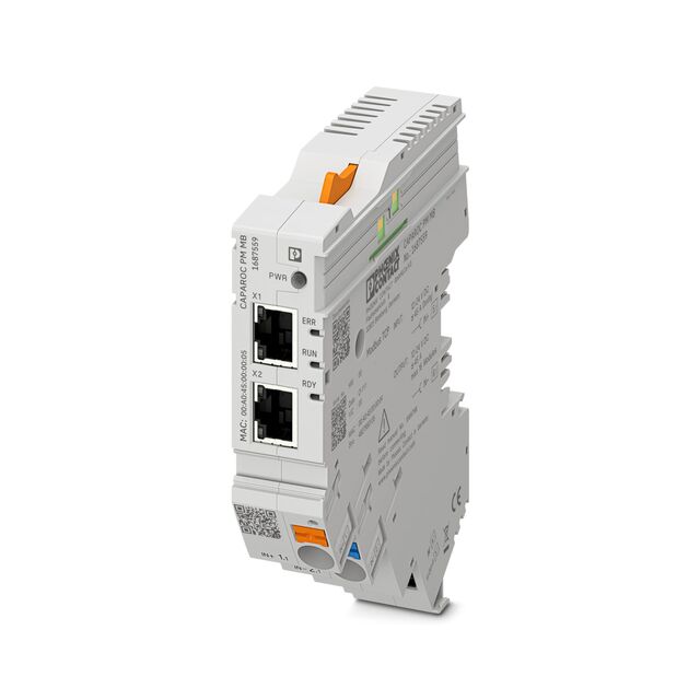
1687559

Phoenix Contact Ltd

[no prices available]

IN STOCK 4
Buy

Reference Designs

RD006

Wurth Elektronik

RD006 - 3 W Dual-output isolated auxiliary supply for communication interfaces and measurement systems

CN0583

Analog Devices Inc.

Multistandard Micropower Verified Smoke Detection System-on-Module

Technical Resources

EVALUATION KITS

EVAL-AD7124-8SDZ

Analog Devices Inc.

$0.00 - * $79.08

IN STOCK 792
Buy
View All