LT8609S Signal Chain Evaluation Board | Synchronous Buck Converter
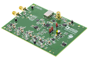
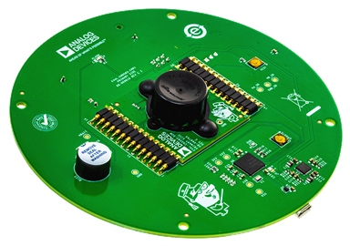
Analog Devices Inc.Demonstration circuit SCP-LT8609S-BEVALZ is a 42V, 2A/3A peak micropower synchronous step-down regula-tor featuring the LT8609S. The demo board is configured for a 5V output from a 5.5V to 42V input.
Like all boards in the Signal Chain Power series, this board is designed to be easily plugged into other SCP boards to form a complete signal chain power system, enabling fast evaluation of low power signal chains. To evaluate this board, some universal SCP hardware is required, namely:
SCP-INPUT-EVALZ
SCP-OUTPUT-EVALZ
SCP-FILTER-EVALZ
SCP-THRUBRD-EVALZ
SCP-1X2BKOUT-EVALZ
SCP-1X5BKOUT-EVALZ
SCP-5X1-EVALZ
To properly evaluate SCP series demo boards, you will need the SCP Configurator companion software. SCP Configurator can help you choose the right board and topology for your design.
Note that the Demo Manual does not cover details important to the operation and configuration regarding the LT8609S. Please refer to the LT8609S datasheet for a complete description of the part.

SSM2305-EVALZ
Analog Devices Inc.The SSM2305 is a fully integrated, high efficiency, Class-Daudio amplifier designed to maximize performance for mobilephone applications. The application circuit requires a minimumof external components and operates from a single 2.5 V to 5.5 Vsupply. It is capable of delivering 2.2 W of continuous outputpower with less than 1% THD + N driving a 4 ? load from a5.0 V supply. It has built-in thermal shutdown and output short-circuitprotection.The SSM2305 features a high efficiency, low noise modulationscheme that does not require external LC output filters. The modulationprovides high efficiency even at low output power. TheSSM2305 operates with 90% efficiency at 1.3 W into 8 ? or 83%efficiency at 2.2 W into 4 ? from a 5.0 V supply and has an SNR of>98 dB. Spread-spectrum pulse density modulation is used toprovide lower EMI-radiated emissions compared with otherClass-D architectures.The SSM2305 has a micropower shutdown mode with a maximumshutdown current of 30 nA. Shutdown is enabled by applyinga Logic 0 to the SD pin. The device also includes pop-and-clicksuppression circuitry. This minimizes voltage glitches at theoutput during turn-on and turn-off, thus reducing audible noiseon activation and deactivation.The fully differential input of the SSM2305 provides excellentrejection of common-mode noise on the input. Input couplingcapacitors can be omitted if the dc input common-mode voltageis approximately VDD/2.The SSM2305 has excellent rejection of power supply noise,including noise caused by GSM transmission bursts and RFrectification. PSRR is typically 60 dB at 217 Hz.The default gain of the SSM2305 is 18 dB, but users can reduce thegain by using a pair of external resistors.The SSM2305 is specified over the commercial temperature range(?40?C to +85?C). It is available in both an 8-lead, 3 mm ? 3 mmlead frame chip scale package (LFCSP) and an 8-lead mini smalloutline package (MSOP). Applications Mobile phones MP3 players Portable gaming Portable electronics Educational toys

SSM6322CP-EBZ
Analog Devices Inc.The SSM6322 is an integrated, dual-channel audio amplifier solution that interfaces directly with audio DAC/CODEC, maximizing the fidelity of high fidelity audio signal chains. The highly efficient design of the SSM6322 delivers outstandingaudio performance while minimizing power dissipation for maximum battery life in portable applications.The SSM6322 features ?121 dB THD + N at 1 kHz, along with very low output noise from 20 Hz to 20 kHz. The low power operation, high peak output current, and high PSRR make the SSM6322 an ideal candidate for applications that require high fidelity audio, high dynamic range, precision, and low power. This highly integrated drive solution also reduces development time while reducing board space and minimizing external components.The SSM6322 is available in a 24-lead LFCSP package. The SSM6322 operates over the industrial temperature of ?40?C to +85?C.Applications High fidelity headphone driver Mobile phones Bluetooth speakers & headphones Gaming Notebooks and Tablets A/V receivers Professional audio equipment Audio test equipment Automobile infotainment system

USB-EA-CONVZ
Analog Devices Inc.The ADuC841/ADuC842/ADuC843are complete smart transducer front ends, that integrates a high performance self-calibrating multichannel ADC, a dual DAC, and an optimized single-cycle 20 MHz 8-bit MCU (8051 instruction set compatible)on a single chip.The ADuC841 and ADuC842 are identical with the exception of the clock oscillator circuit; the ADuC841 is clocked directly from an external crystal up to 20 MHz whereas the ADuC842 uses a 32 kHz crystal with an on-chip PLL generating aprogrammable core clock up to 16.78 MHz.The ADuC843 is identical to the ADuC842 except that the ADuC843 has no analog DAC outputs.The microcontroller is an optimized 8052 core offering up to 20 MIPS peak performance. Three different memory options are available offering up to 62 kBytes of nonvolatile Flash/EE program memory. Four kBytes of nonvolatile Flash/EE data memory, 256 bytes RAM, and 2 kBytes of extended RAM arealso integrated on-chip. The parts also incorporate additional analog functionality with two 12-bit DACs, power supply monitor, and a band gap reference. On-chip digital peripherals include two 16-bit ?-?. DACs, a dual output 16-bit PWM, a watchdog timer, a time interval counter, three timers/counters, and three serial I/O ports (SPI, I2C, and UART).On the ADuC812 and the ADuC832, the I2C and SPI interfaces share some of the same pins. For backwards compatibility, this is also the case for the ADuC841/ADuC842/ADuC843.However, there is also the option to allow SPI operate separately on P3.3, P3.4, and P3.5, while I2C uses the standard pins. The I2C interface has also been enhanced to offer repeated start, general call, and quad addressing.On-chip factory firmware supports in-circuit serial download and debug modes (via UART) as well as single-pin emulation mode via the EA pin.Applications Optical networking?laser power control Base station systems Precision instrumentation, smart sensors Transient capture systems DAS and communications systems
DC2242A
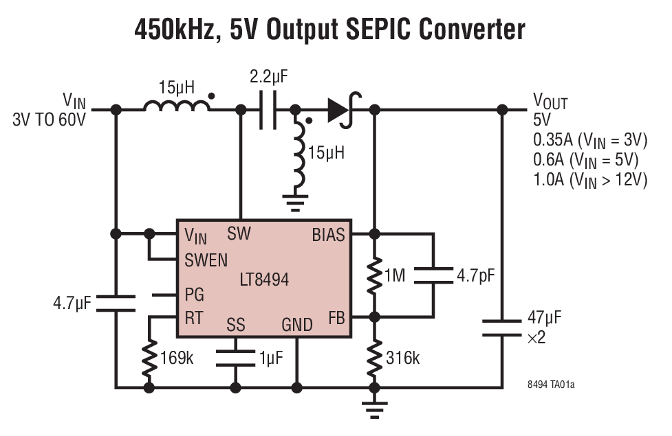
Analog Devices Inc.The LT8494 is an adjustable frequency (250kHz to 1.5MHz) monolithic switching regulator. Quiescent current can be less than 7?A when operating and is ~0.3?A when SWEN is low. The LT8494 can be configured as either a SEPIC, boost or flyback converter.The low ripple Burst Mode operation maintains high efficiency at low output current while keeping output ripple below 10mV. Dual supply pins (VIN and BIAS) allow the part to automatically operate from the most efficient supply. Input supply voltage can be up to 60V for SEPIC topologies and up to 32V (with ride-through up to 60V) for boost and flyback topologies. After start-up, battery life is extended since the part can draw current from its output (BIAS) even when VIN voltage drops below 2.5V.Using a resistor divider on the SWEN pin provides a programmable undervoltage lockout (UVLO) for the converter. A power good flag signals when VOUT reaches 92% of the programmed output voltage.Additional features such as frequency foldback and soft-start are integrated. The LT8494 is available in 20-lead QFN and 20-lead TSSOP packages with exposed pads for low thermal resistance. Fault tolerance in the TSSOP allows for adjacent pin shorts or an open without raising the output voltage above its programmed value.Applications Automotive ECU Power Power for Portable Products Industrial Supplies

LT3922 Demo Board | Synchronous Boost LED Driver, 4V ≤ VIN ≤ 28V, VLED = 34V @ Up to 330mA, 2MHz fSWITCH
Analog Devices Inc.Demonstration circuit DC2247A is a synchronous 2MHz boost LED driver featuring the LT®3922. The LT3922 features a low EMI Silent Switcher architecture and an optional spread spectrum frequency modulation (SSFM) that further reduces EMI. It has a 2A/36V internal power switch, but the demo board has been configured to use a 4V to 28V input and thus has input overvoltage lockout set at 28V. It drives a single string of LEDs at 330mA up to 34V when the input voltage is between 7V and 28V.
DC2247A comes with low EMI features including optimized layout, SSFM, and input and output filters. It passes CISPR 25 class 5 conducted and radiated EMI. The LT3922 is protected against both open and short LED conditions and reports these faults. It also includes thermal shutdown.
DC2251A
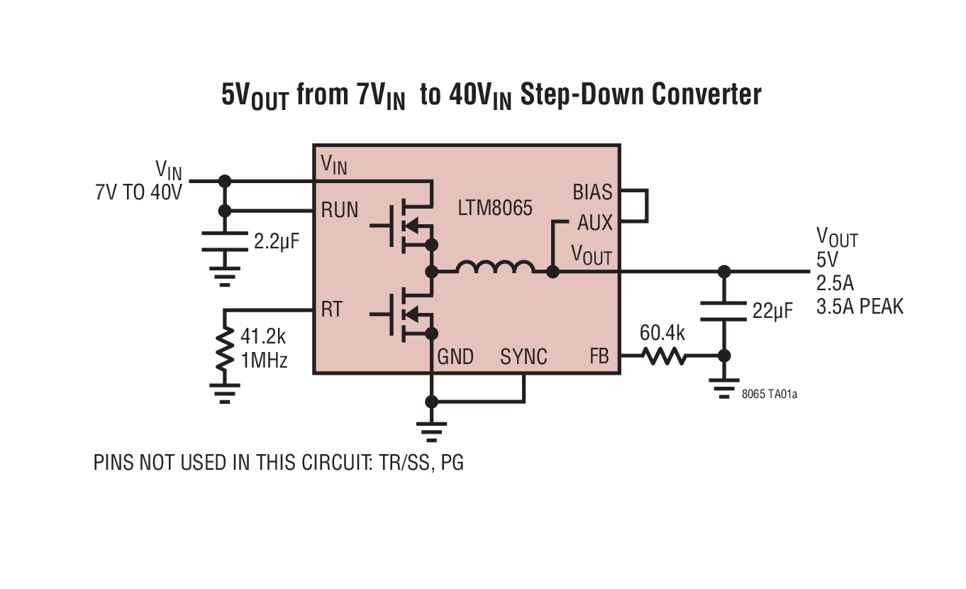
Analog Devices Inc.The LTM8065 is a 40VIN, 3.5A peak, 2.5A continuous step-down ?Module? (power module) regulator. Included in the package are the switching controller, power switches, inductor and all support components. Operating over an input voltage range of 3.4V to 40V, the LTM8065 supports an output voltage range of 0.97V to 18V and a switching frequency range of 200kHz to 3MHz, each set by a single resistor. Only the input and output filter capacitors are needed to finish the design.The low profile package enables utilization of unused space on the bottom of PC boards for high density point of load regulation. The LTM8065 is packaged in a thermally enhanced, compact over-molded ball grid array (BGA) package suitable for automated assembly by standard surface mount equipment. The LTM8065 is RoHS compliant.Applications Automotive Battery Regulation Power for Portable Products Distributed Supply Regulation Industrial Supplies Wall Transformer Regulation
DC2254A-B
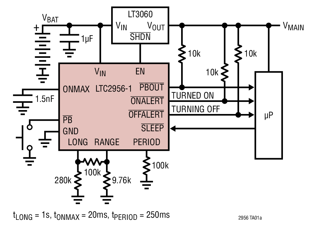
Analog Devices Inc.The LTC2956 is a micropower, wide input voltage range, configurable wake-up timer with pushbutton control. It periodically wakes up and turns on a connected system to perform tasks like monitoring temperature or capturing images. After completing the task, the LTC2956 turns the system off to conserve power.The wake-up timer period can be adjusted from 250ms to 39 days using configuration resistors. The system awake time can be controlled by the input pulse at the SLEEP pin or adjusted by the capacitor at the ONMAX pin. The LTC2956 operates over a wide supply input range from 1.5V to 36V. The low 800nA quiescent current suits battery powered applications.The pushbutton input allows the user to shutdown, turn on or reset the wake-up timer. With the timer in shutdown, the quiescent current drops to 300nA. The LTC2956 also provides three status outputs to indicate mode transitions and pushbutton events. Two versions are available for applications requiring either positive or negative enable polarities.Applications Heartbeat Timers Periodic Wake-Up Control Portable and Battery-Powered Equipment Intervalometers Data Acquisition
DC2266A
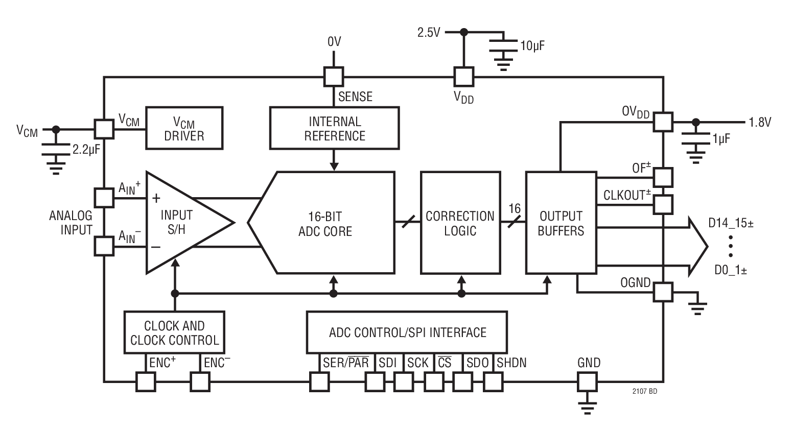
Analog Devices Inc.The LTC2107 is a 16-bit, 210Msps high performance ADC. The combination of high sample rate, low noise and high linearity enable a new generation of digital radio designs. The direct sampling front-end is designed specifically for the most demanding receiver applications such as software defined radio and multi-channel GSM base stations. The AC performance includes, SNR = 80dBFS, SFDR = 98dBFS. Aperture jitter = 45fsRMS allows direct sampling of IF frequencies up to 500MHz with excellent performance.Features such as internal dither, a PGA front-end and digital output randomization help maximize performance. Modes of operation can be controlled through a 3-wire serial interface (SPI).The double data rate (DDR) low voltage differential (LVDS) digital outputs help reduce digital line count and enable space saving designs.Applications Software Defined Radios Military Radio and RADAR Cellular Base Stations Spectral Analysis Imaging Systems ATE and Instrumentation

DC2268A-C
Analog Devices Inc.The LTM4628 is a complete dual 8A output switching mode DC/DC power supply and can be easily configured to provide a single 2-phase 16A output. Included in the package are the switching controller, power FETs, inductor, and all supporting components. Operating from an input voltage range of 4.5V to 26.5V, the LTM4628 supports two outputs each with an output voltage range of 0.6V to 5.5V, set by a single external resistor. Its high efficiency design delivers 8A continuous current for each output. Only a few input and output capacitors are needed.The device supports frequency synchronization, multiphase operation, Burst Mode operation and output voltage tracking for supply rail sequencing. It has an on-board temperature diode for device temperature monitoring. High switching frequency and a current mode architecture enable a very fast transient response to line and load changes without sacrificing stability.Fault protection features include overvoltage and overcurrent protection. The power module is offered in space saving and thermally enhanced 15mm ? 15mm ? 4.32mm LGA and 15mm ? 15mm ? 4.92mm BGA packages. The LTM4628 is available with SnPb (BGA) or RoHS compliant terminal finish.Applications Telecom and Networking Equipment Storage and ATCA Cards Industrial Equipment
DC2268A-G
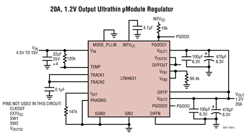
Analog Devices Inc.The LTM4631 is a dual 10A or single 20A output switching mode step-down DC/DC ?Module? (power module) regulator. Included in the package are the switching controller, power FETs, inductors and all supporting components. Operating from an input voltage range of 4.5V to 15V, the LTM4631 supports two outputs each with an output voltage range of 0.6V to 1.8V, each set by a single external resistor. Its high efficiency design delivers up to 10A continuous current for each output. Only a few input and output capacitors are needed.The device supports frequency synchronization, multiphase operation, Burst Mode operation and output voltage tracking for supply rail sequencing and has an onboard temperature diode for device temperature monitoring. High switching frequency and a current mode architecture enable a very fast transient response to line and load changes without sacrificing stability.Fault protection features include overvoltage and overcurrent protection. The LTM4631 is offered in an ultrathin 16mm ? 16mm ? 1.91mm LGA and 16mm x 16mm x 2.51mm BGA packages. The LTM4631 is available with SnPb (BGA) or ROHS compliant terminal finish.Applications Telecom and Networking Equipment Storage and ATCA Cards Industrial Equipment
DC2276A
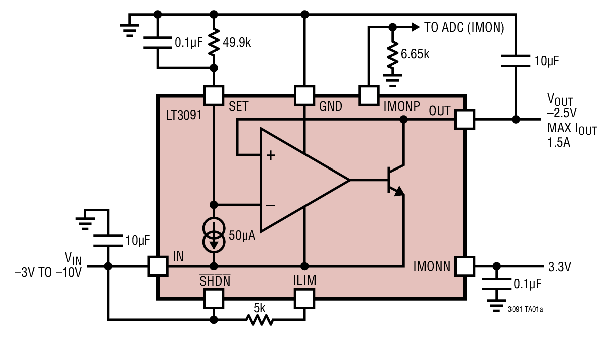
Analog Devices Inc.The LT3091 is a 1.5A, low dropout negative linear regulator that is easily paralleled to increase output current or spread heat on surface mounted boards. Designed with a precision current reference followed by a high performance rail-to-rail voltage buffer, this regulator finds use in applications requiring precision output, high current with no heat sink, output adjustability to zero and low dropout voltage. The device can also be configured as a 3-terminal floating regulator.The LT3091 features fast transient response, high PSRR and output noise as low as 18?VRMS. The LT3091 generates a wide output voltage range (0V to ?32V) while maintaining unity gain operation. This yields virtually constant bandwidth, load regulation, PSRR and noise, independent of the programmed output voltage.The LT3091 supplies 1.5A at a typical dropout voltage of 300mV. Operating quiescent current is nominally 1.2mA and drops to

LTC4281 Demo Board | 12V, 50A Hot Swap Controller with Telemetry [Requires DC1613]
Analog Devices Inc.Demonstration circuit 2278A features the LTC4281 hot swap controller. The LTC4281 is well suited to high power applications because the precise monitoring capability and accurate current limiting reduces the extremes in which both loads and power supplies must safely operate. Non-volatile configuration allows for flexibility in the autonomous generation of alerts and response to faults.
DC2290A-C
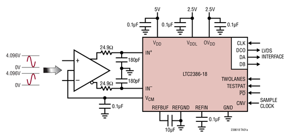
Analog Devices Inc.The LTC2386-18 is a low noise, high speed, 18-bit 10Msps successive approximation register (SAR) ADC ideally suited for a wide range of applications. The combination of excellent linearity and wide dynamic range makes the LTC2386-18 ideal for high speed imaging and instrumentation applications. No-latency operation provides a unique solution for high speed control loop applications. The very low distortion at high input frequencies enables communications applications requiring wide dynamic range and significant signal bandwidth.To support high speed operation while minimizing the number of data lines, the LTC2386-18 features a serial LVDS digital interface. The LVDS interface has one-lane and two-lane output modes, allowing the user to optimize the interface data rate for each application.Applications High Speed Data Acquisition Imaging Communications Control Loops Instrumentation ATE
DC2290A-E
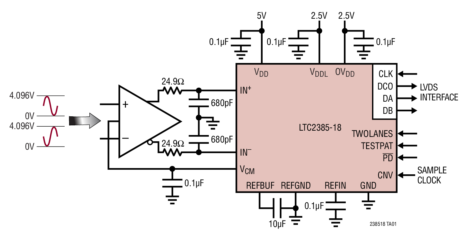
Analog Devices Inc.The LTC2385-18 is a low noise, high speed, 18-bit 5Msps successive approximation register (SAR) ADC ideally suited for a wide range of applications. The combination of excellent linearity and wide dynamic range makes the LTC2385-18 ideal for high speed imaging and instrumentation applications. No-latency operation provides a unique solution for high speed control loop applications. The very low distortion at high input frequencies enables communications applications requiring wide dynamic range and significant signal bandwidth.To support high speed operation while minimizing the number of data lines, the LTC2385-18 features a serial LVDS digital interface. The LVDS interface has one-lane and two-lane output modes, allowing the user to optimize the interface data rate for each application.Applications High Speed Data Acquisition Imaging Communications Control Loops Instrumentation ATE

DC2293A-A
Analog Devices Inc.The LTC2933 is an EEPROM configurable voltage supervisor which can simultaneously monitor up to six power supply voltage inputs. Each voltage detector offers I2C programmable over/undervoltage thresholds in various ranges and increments.Two general purpose inputs (GPI) can be configured as programmable manual reset (MR), UV disable (UVDIS), margin (MARG) or auxiliary comparator (AUXC) inputs. Three general purpose pins (GPIO) can be configured for input or output operation. When configured as an input, a GPIO pin can be mapped to any other GPIO configured as output. The GPIO pins can also be configured as ALERT or fault outputs. Faults can be configured with programmable delay-on-release times. Output type and polarity are also configurable.Status and history registers log faults and can be polled via the I2C interface. A fault log snapshot is also backed up in internal EEPROM. All parameters are programmable via the I2C interface. Configuration EEPROM supports autonomous operation without additional software.Applications High Availability Computer Systems Network Servers Telecom Equipment Data Storage
LT8570EDD-1 Demo Board | Boost, 5V ≤ VIN ≤ 10V, VOUT = 12V @ 60mA
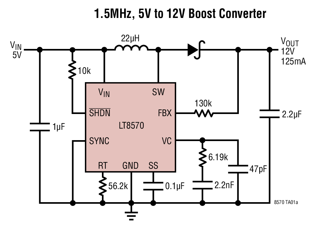
Analog Devices Inc.Demonstration circuits 2297A-A and 2297A-B feature the LT8570 and LT8570-1 in a boost configuration. These demo circuits demonstrate small size and low component count. Both converters are designed to convert a 5V to 10V source to 12V. The DC2297A-A (LT8570) provides 125mA of output current, and the DC2297A-B (LT8570-1) provides 60mA of output current.

DC2299A-B
Analog Devices Inc.The LTC3890-1 is a high performance dual step-down switching regulator DC/DC controller that drives all N-channel synchronous power MOSFET stages. A constant frequency current mode architecture allows a phase-lockable frequency of up to 850kHz. Power loss and supply noise are minimized by operating the two controller output stages out-of-phase.The 50?A no-load quiescent current extends operating life in battery-powered systems. OPTI-LOOP? compensation allows the transient response to be optimized over a wide range of output capacitance and ESR values. A wide 4V to 60V input supply range encompasses a wide range of intermediate bus voltages and battery chemistries.Independent TRACK/SS pins for each controller ramp the output voltages during start-up. Current foldback limits MOSFET heat dissipation during short-circuit conditions. The PLLIN/MODE pin selects among Burst Mode operation, pulse-skipping mode, or continuous conduction mode at light loads.For a leadless 32-pin QFN package with additional features of adjustable current limit, clock out, phase modulation and two PGOOD outputs, see the LTC3890 data sheet. LTC3890 LTC3890-1 LTC3890-2 LTC3890-3 Adjustable Current Limit Limit Yes No Yes No CLKOUT/PHASMD for Multiphase Operation Yes No Yes No Number of PGood Outputs 2 1 2 1 OVP ? Bottom Gate Crowbar Yes Yes No No Current Limit Foldback Yes Yes No No Light Load Operation when Synced to External Clock Forced Continuous Forced Continuous Pulse Skipping Pulse Skipping SENSE Pins Common Mode Range Common Mode < 0.5V Requires VFB < 0.65V Common Mode < 0.5V Requires VFB < 0.65V Not Dependant on VFB. Easy to make a non-synchronous Boost or SEPIC Not Dependant on VFB. Easy to make a non-synchronous Boost or SEPIC Package 5 ? 5 QFN-32 SSOP-28 5 ? 5 QFN-32 SSOP-28 Applications Automotive Always-On Systems Battery Operated Digital Devices Distributed DC Power Systems
DC2303A-B
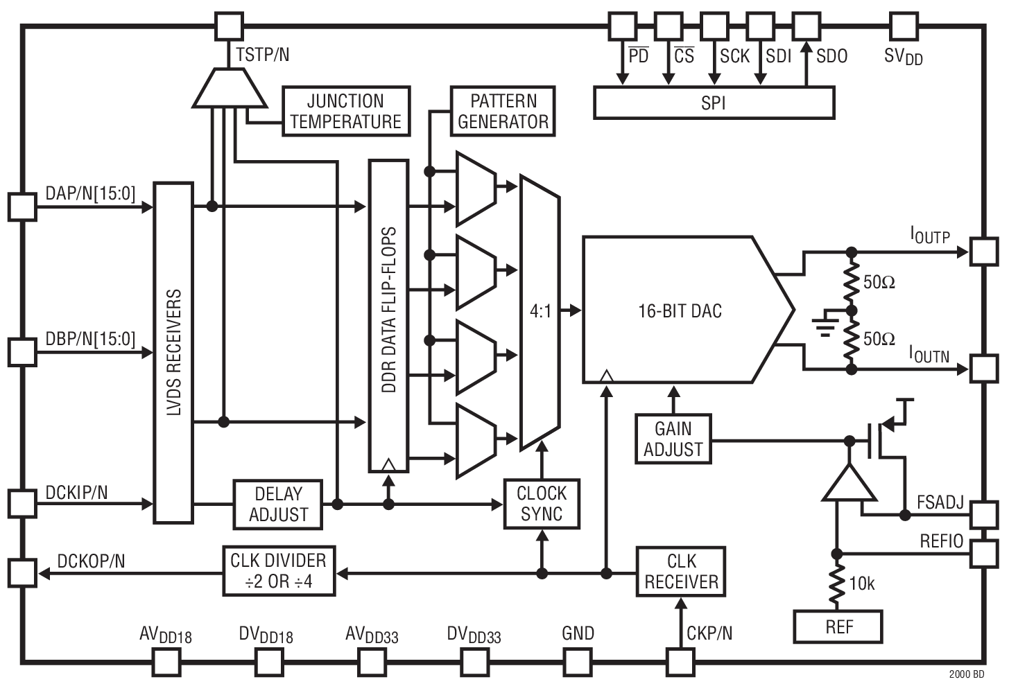
Analog Devices Inc.The LTC2000 is a family of 16-/14-/11-bit 2.5Gsps current steering DACs with exceptional spectral purity.The single (1.25Gsps mode) or dual (2.5Gsps mode) port source synchronous LVDS interface supports data rates of up to 1.25Gbps using a 625MHz DDR data clock, which can be either in quadrature or in phase with the data. An internal synchronizer automatically aligns the data with the DAC sample clock.Additional features such as pattern generation, LVDS loopout and junction temperature sensing simplify system development and testing.A serial peripheral interface (SPI) port allows configuration and read back of internal registers. Operating from 1.8V and 3.3V supplies, the LTC2000 consumes 2.2W at 2.5Gsps and 1.3W at 1.25Gsps.Applications Broadband Communication Systems DOCSIS CMTS Direct RF Synthesis Radar Instrumentation Automatic Test Equipment

DC2303A-D
Analog Devices Inc.The LTC2000A is a family of 16-/14-/11-bit 2.7Gsps current steering DACs with exceptional spectral purity.The single (1.35Gsps mode) or dual (2.7Gsps mode) port source synchronous LVDS interface supports data rates of up to 1.35Gbps using a 675MHz DDR data clock, which can be either in quadrature or in phase with the data. An internal synchronizer automatically aligns the data with the DAC sample clock.Additional features such as pattern generation, LVDS loopout and junction temperature sensing simplify system development and testing.A serial peripheral interface (SPI) port allows configuration and read back of internal registers. Operating from 1.86V and 3.3V supplies, the LTC2000A consumes 2.41W at 2.7Gsps and 1.43W at 1.35Gsps.Applications Broadband Communication Systems DOCSIS CMTS Direct RF Synthesis Radar Instrumentation Automatic Test Equipment