
LT5568EUF | 900MHz I/Q Modulator
Analog Devices Inc.DC966A: Demo Board for the LT5568 700MHz to 1050MHz High Linearity Direct Quadrature Modulator.
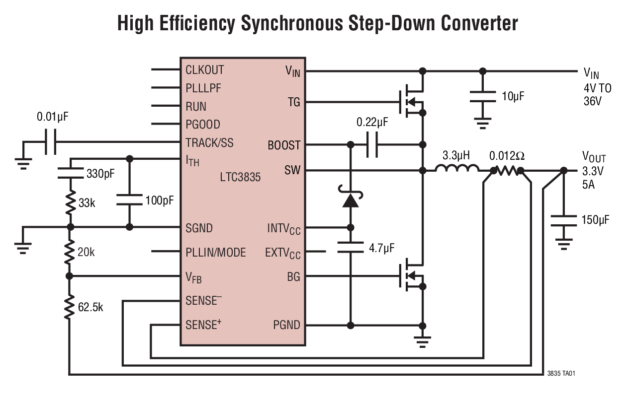
LTC3835EFE Demo Board | 4.5V ≤ VIN ≤ 36V, VOUT = 3.3V @ 5A
Analog Devices Inc.Demonstration circuit 967B is a single output high frequency step-down DC/DC controller featuring the low quiescent current LTC3835 in a 20-pin exposed pad TSSOP package. The DC967B is designed to generate a regulated 3.3V@5A output from 4.5V to 36V input voltage.

LTC2241CUP-10 | LVDS OUT, VCC = 2.5V, 210Msps, 10-Bit, 10MHz < AIN < 250MHz (Requires DC890 & LVDS_XFMR)
Analog Devices Inc.DC997B-E - Demo Board for the LTC2241-10 10-Bit, 210Msps ADC.

LTC4261 –48V Hot Swap w/ADC (Requires DC590)
Analog Devices Inc.DC998A - Demo Board for the LTC4261 Negative Voltage Hot Swap Controllers with ADC and I2C Monitoring.

EK1HMC8200LP5M
Analog Devices Inc.The HMC8200LP5ME is a highly integrated intermediatefrequency (IF) transmitter chip that converts the industrystandard 300 MHz to 400 MHz IF input signals to an 800 MHz to4000 MHz single-ended radio frequency (RF) signal at its output.The IF transmitter chip is housed in a compact 5 mm ? 5 mmLFCSP package and supports complex modulations up to1024 QAM. The HMC8200LP5ME simultaneously reduces thedesign complexity of traditional microwave radios while realizingsignificant size and cost improvements. With IF input powerranges from ?31 dBm to +4 dBm, the HMC8200LP5MEprovides 35 dB of digital gain control in 1 dB steps and ananalog voltage gain amplifier (VGA) continuously controls thetransmitter output power from ?20 dBm to +5 dBm.The device also features three integrated power detectors. Thefirst detector (LOG_IF) can be utilized to monitor the IF inputpower. The second detector (SLPD_OUT) is a square law powerdetector that monitors the power entering the mixer. The thirdpower detector (LOG_RF) is used to monitor the output power,which can be used for fine output power adjustment.Applications Point to point communications Satellite communications Wireless microwave backhaul systemsPlease also view complementary product HMC8100, Intermediate Frequency Receiver 800 MHz - 4000 MHz

EK1HMC832ALP6G
Analog Devices Inc.The HMC832A is a 3.3 V, high performance, wideband, fractional-N, phase-locked loop (PLL) that features an integrated voltage controlled oscillator (VCO) with a fundamental frequency of 1500 MHz to 3000 MHz and an integrated VCO output divider (divide by 1, 2, 4, 6, ? 62) that enables the HMC832A to generate continuous frequencies from 25 MHz to 3000 MHz. The integrated phase detector (PD) and ?-? modulator, capable of operating at up to 100 MHz, permit wider loop bandwidths and faster frequency tuning with excellent spectral performance.Industry leading phase noise and spurious performance, across all frequencies, enable the HMC832A to minimize blocker effects, and to improve receiver sensitivity and transmitter spectral purity. A low noise floor (?160 dBc/Hz) eliminates any contribution to modulator/mixer noise floor in transmitter applications.The HMC832A is footprint compatible to the market leading HMC830 PLL with an integrated VCO. It features 3.3 V supply and an innovative programmable performance technology that enables the HMC832A to tailor current consumption and corresponding noise floor performance to individual applications by selecting either a low current consumption mode or a high performance mode for an improved noise floor performance.Additional features of the HMC832A include 12 dB of RF output gain control in 1 dB steps; an output mute function to automatically mute the output during frequency changes when the device is not locked; selectable output return loss; programmable differential or single-ended outputs, with the ability to select either output in single-ended mode; and a ?-? modulator exact frequency mode that enables users to generate output frequencies with 0 Hz frequency error; and a register configurable 3.3 V or 1.8 V serial port interface (SPI).Applications Cellular infrastructure Microwave radios WiMax, WiFi Communications test equipment CATV equipment DDS replacement Military Tunable reference sources for spurious-free performance

EKIT01-HMC1023LP5
Analog Devices Inc.The HMC1023 is a 6th order, programmable bandwidth, fully calibrated, dual low pass filter. It features programmable 0 or 10 dB gain and supports arbitrary bandwidths from 5 MHz to 72 MHz. When calibrated, the bandwidth is accurate to +/-2.5%. Built-in filter bypass option enables wider bandwidths while maintaining programmed gain and common mode control settings.Integrated ADC driver, programmable input impedance, and adjustable output common mode voltage from 0.9 V to 3 V with 2 Vppd signal, or lower than 0.9 V common mode with lower signal swing enables simple interface while achieving maximum performance. Programmable bias settings enable performance/power dissipation trade-off optimized for each application.Filter calibration is accomplished with any reference clock rate from 20 to 80 MHz. One time programmable (OTP) memory offers unsurpassed flexibility allowing the user ?set and forget? parameters like gain and bandwidth setting.Housed in a compact 5x5 mm SMT QFN package, the HMC1023 is pin and register compatible to the existing HMC900 programmable bandwidth Low Pass Filter. It requires minimal external components and provides a low cost alternative to more complicated switched discrete filter architectures.The 6th order Butterworth transfer function delivers superior stop band rejection while maintaining both a flat passband and minimal group delay variation.Applications Baseband filtering before or after?data converters for point-to-point fixed?wireless and cellular infrastructure?transceivers Software defined radio applications Anti-aliasing and reconstruction filters Test and measurement equipment ADC driver applications

EKIT01-HMC1032LP6G
Analog Devices Inc.The HMC1032LP6GE is a low-noise, wide-band clock generator IC with a fractional-N Phase Locked Loop (PLL) that features an integrated Voltage Controlled Oscillator (VCO). The device provides differential clock outputs between 125 and 350 MHz range. The HMC1032LP6GE features low noise Phase Detector (PD) and Delta-Sigma modulator, capable of operating at up to 100 MHz, permit wider loop-bandwidths with excellent spectral performance.The HMC1032LP6GE features industry leading phase noise and jitter performance, across the operating range, that enable it to improve link level jitter performance, Bit-Error-Rates (BER) and eye diagram metrics. The superior noise floor (

EKIT01-HMC1044LP3E
Analog Devices Inc.The HMC1044LP3E is a programmable bandwidth LPF (Low Pass Filter) targeted at all applications that use quadrature modulators and/or demodulators. The HMC1044LP3E filters out LO harmonics and ensures little or no LO contribution to modulator sideband rejection or demodulator image rejection performance.Although targeted at LO filtering applications, the HMC1044LP3E can be used to filter all RF harmonics such as the ones generated by amplifiers.The HMC1044LP3E offers a choice of 16 programmable bands, optimized for high and low cellular bands ranging from 1 to 3 GHz, making the a truly wideband part compatible with wideband PLLs with Integrated VCOs and wideband quadrature modulators and demodulators. It enables wideband multi-standard, multi-carrier designs that are field configurable on-the-fly for each individual application.The HMC1044LP3E is packaged in a compact 3x3 mm QFN leadless package.APPLICATIONS Filtering LO Harmonics to Reduce Modulator Sideband?Rejection & Demodulator?Image Rejection Amplifier Harmonic Filtering RF Filtering

EKIT01-HMC778LP6CE
Analog Devices Inc.The HMC778LP6CE is a fully functioned Fractional-N Phase-Locked-Loop (PLL) Frequency Synthesizer with an integrated Voltage Controlled Oscillator (VCO). The input reference frequency range is DC to 350 MHz while the advanced delta-sigma modulator design in the fractional synthesizer allows both ultra-fine step sizes and very low spurious products. The highly integrated structure provides excellent phase noise performance over temperature, shock and process. In addition, the HMC778LP6CE offers frequency sweep and modulation features, external triggering, double-buffering, exact frequency control, phase modulation and more. The HMC778LP6CE is packaged in a leadless QFN 6 x 6 mm surface mount package.For theory of operation and register map refer to the 'PLLs w/ Integrated VCO - Microwave VCOs' Operating Guide.Applications VSAT Radio Microwave Point-To-Point Radios Test Equipment & Industrial Control Military End-Use Phased Array Applications FMCW Radar Systems

EKIT01-HMC829LP6GE
Analog Devices Inc.The HMC829LP6GE is a low noise, wide band, Fractional-N Phase-Locked-Loop (PLL) that features an integrated Voltage Controlled Oscillator (VCO ) with a fundamental frequency of 2800 MHz - 4200 MHz, and an integrated VCO Output Divider (divide by 1/2/4/6.../60/62), that together allow the HMC829LP6GE to generate frequencies from 45 MHz to 1050 MHz, from 1400 MHz to 2100 MHz, and from 2800 MHz to 4200 MHz. The integrated Phase Detector (PD) and delta-sigma modulator, capable of operating at up to 100 MHz, permit wider loop-bandwidths with excellent spectral performance.For theory of operation and register map refer to the 'PLLs w/ Integrated VCO - Microwave VCOs' Operating Guide.Applications Cellular/4G, WiMax Infrastructure Repeaters and Femtocells Communications Test Equipment CATV Equipment Phased Array Applications DDS Replacement Very High Data Rate Radios

EV1HMC1095LP4
Analog Devices Inc.The HMC1095LP4E is a broadband 6-bit GaAs IC Digital Attenuator in a low cost leadless SMT package. This versatile digital attenuator incorporates off-chip AC ground capacitors for near DC operation, making it suitable for a wide variety of RF and IF applications. The dual mode control interface is CMOS/TTL compatible, and accepts either a three wire serial input or a 6 bit parallel word. The HMC1095LP4E also features a user selectable power up state and a serial output port for cascading other Hittite serial controlled components. The HMC1095LP4E is housed in a RoHS compliant 4?4 mm QFN leadless package, and requires no external matching components.APPLICATIONS CATV/Satellite Set Top Boxes CATV Modems CATV Infrastructure Data Network Equipment

EV1HMC1096LP3
Analog Devices Inc.The HMC1096LP3E is a x2 active broadband frequency multiplier utilizing GaAs pHEMT technology in a leadless RoHS compliant Low Stress Injection Molded Plastic SMT package. When driven by a 0 dBm signal, the multiplier provides+12 dBm typical output power from 3.8 to 5.6 GHz. The Fo and 3 Fo isolations are +22 dBc with respect to the output signal level. This frequency multiplier features DC blocked I/Os, and is ideal for use in LO multiplier chains for Point-to-Point & VSAT radios yielding reduced parts count vs. traditional approaches. The HMC1096LP3E is compatible with surface mount manufacturing techniques.Applications Point-to-Point & VSAT Radios Test Instrumentation Military & Space

EV1HMC1113LP5
Analog Devices Inc.The HMC1113LP5E is a compact GaAs MMIC I/Q downconverter in a leadless 5 x 5 mm low stress injection molded plastic surface mount package. This device provides a small signal conversion gain of 12 dB with a noise figure of 1.8 dB and 25 dBc of image rejection. The HMC1113LP5E utilizes an LNA followed by an image reject mixer which is driven by an LO buffer amplifier. The image reject mixer eliminates the need for a filter following the LNA, and removes thermal noise at the image frequency. I/Q mixer outputs are provided and an external 90? hybrid is needed to select the required sideband. The HMC1113LP5E is a much smaller alternative to hybrid style image reject mixer downconverter assemblies, and it eliminates the need for wire bonding by allowing the use of surface mount manufacturing techniques.Applications Point-to-Point &?Point-to-Multi-Point Radio Military Radar, EW & ELINT Satellite Communications Maritime & Mobile Radios

EV1HMC1114PM5
Analog Devices Inc.TThe HMC1114PM5E is a gallium nitride (GaN), broadband power amplifier delivering >10 W (up to 42 dBm) typical with up to 55% power added efficiency (PAE) across an instantaneous bandwidth range of 2.7 GHz to 3.8 GHz, at an input power (PIN) of 18 dBm. The gain flatness is The HMC1114PM5E is ideal for pulsed or continuous wave (CW) applications, such as wireless infrastructure, radars, public mobile radios, and general-purpose amplification.Applications Extended battery operation for public mobile radios Power amplifier stage for wireless infrastructure Test and measurement equipment Commercial and military radars General-purpose transmitter amplification

EV1HMC1121LP6G
Analog Devices Inc.The HMC1121 is a three-stage, gallium arsenide (GaAs), pseudomorphic high electron mobility transfer (pHEMT), monolithic microwave integrated circuit (MMIC), 4 W power amplifier with an integrated temperature compensated on-chip power detector that operates between 5.5 GHz and 8.5 GHz. The HMC1121 provides 28 dB of gain, 44 dBm output IP3, and 36.5 dBm of saturated output power at 30% PAE from a 7 Vpower supply. The HMC1121 exhibits excellent linearity and it is optimized for high capacity, point to point and point to multipoint radio systems. The amplifier configuration and high gain make it an excellent candidate for last stage signal amplification preceding the antenna. Ideal for supporting higher volume applications, the HMC1121 is provided in a 40-lead LFCSP package.Applications Point to point radios Point to multipoint radios? Very small aperture terminals (VSATs) and satellite?communications (SATCOMs) Military electronic warfare ?(EW) and electronic counter measures (ECM)

EV1HMC1160LP5
Analog Devices Inc.The HMC1160 is a MMIC voltage controlled oscillator that integrates a resonator, a negative resistance device, and a varactor diode, and features a half frequency output.Because of the monolithic construction of the oscillator, output power and phase noise performance are excellent over temperature.Power output is 12 dBm typical from a 5 V supply voltage. The voltage controlled oscillator is housed in a RoHS compliant SMT package and requires no external matching components.APPLICATIONS Point to point and multipoint radio Test equipment and industrial controls VSAT

EV1HMC1165LP5
Analog Devices Inc.The HMC1165 is a monolithic microwave integrated circuit (MMIC), voltage controlled oscillator (VCO) that integrates a resonator, a negative resistance device, and a varactor diode, and features a half frequency output. Because of the monolithic construction of the oscillator, the output power and phase noise performance are excellent over temperature.The output power is 8 dBm typical from a 5 V supply voltage. The VCO is housed in a RoHS-compliant LFCSP and requires no external matching components.Applications Point to point and multipoint radios? Test equipment and industrial controls? Very small aperture terminals (VSATs)?

EV1HMC1168LP5
Analog Devices Inc.The HMC1168 is a monolithic microwave integrated circuit(MMIC), voltage controlled oscillator (VCO) that integrates aresonator, a negative resistance device, and a varactor diode,and features a half frequency output.Because of the monolithic construction of the oscillator, theoutput power and phase noise performance are excellent overtemperatureThe output power is 10 dBm typical from a 5 V supply voltage.The VCO is housed in a RoHS compliant LFCSP and requiresno external matching components.Applications Point to point and multipoint radios? Test equipment and industrial controls? Very small aperture terminals (VSATs)?

EV1HMC273AMS10G
Analog Devices Inc.The HMC273AMS10G(E) is a general purposebroadband 5-Bit positive control GaAs IC digitalattenuator in a 10 lead MSOP plastic package.Covering 0.7 to 3.8 GHz, the insertion loss is typicallyless than 3 dB. The attenuator bit values are1 (LSB), 2, 4, 8, and 16 dB for a total attenuationof 31 dB. Accuracy is excellent at ?0.2 dB typicalwith an IIP3 of up to +46 dBm. Five bit control voltageinputs, toggled between 0 and +3 to +5 volts, areused to select each attenuation state. A single Vddbias of +3 to +5 volts applied through an external5K Ohm resistor is required.Applications Cellular; UMTS/3G infrastructure ISM, MMDS, WLAN, WiMAX Microwave radio & VSAT Test equipment and sensors


