
EV1HMC891ALP5
Analog Devices Inc.The HMC891ALP5E is a monolithic microwave integrated circuit (MMIC) band-pass filter that features a user-selectablepass band frequency. The 3 dB filter bandwidth is approximately 9% and the 20 dB filter bandwidth is approximately 23%. Thecenter frequency (fCENTER) can be varied between 1.95 GHz and 3.4 GHz by applying an analog tune voltage between 0 V and 14 V.This tunable filter can be used as a smaller alternative to physically large switched filter banks and cavity tuned filters.The HMC891ALP5E has excellent microphonics due to the monolithic design, and provides a dynamically adjustablesolution in advanced communications applications.ApplicationsTesting and measurement equipmentMilitary radar and electronic warfare/electronic counter measure (ECM)Satellite communication and spaceIndustrial and medical equipment
MAX5391NEVMINIQU+
Analog Devices Inc.Digital Potentiometer Development Tools Eval Kit/System MAX5386M, MAX5388, MAX5391, and MAX5393 (Dual 256-Tap,Volatile, Low-Voltage Linear Taper Digital Potentiometers)

LTC3852EUDD Demo Board | 2.7V ≤ VIN ≤ 5.5V, VOUT = 1.5V @ 15A
Analog Devices Inc.Demonstration circuit 1270A is a low input voltage, high efficiency synchronous buck DC/DC controller that features the LTC3852EUDD. With a 2.7V to 5.5V input range. It can supply 15A maximum load current at 1.5V output. The integrated charge pump provides 5V to the LTC3852’s control logic and gate drives, supporting a wide selection of logic-level N-channel power MOSFETs with high efficiency.

LTC3854EDDB Demo Board | 4.5V ≤ VIN ≤ 14V, VOUT = 1.5V @ 15A
Analog Devices Inc.Demonstration circuit 1271 is a small foot print, high efficiency synchronous buck converter with 4.5V to 14V input range. It can supply 15A maximum load current at 1.5V output. The demo board features the LTC3854EDDB controller. The controller features a 400kHz constant frequency current mode architecture and allows RSENSE or DCR inductor current sensing. The demo board is configured using RSENSE.
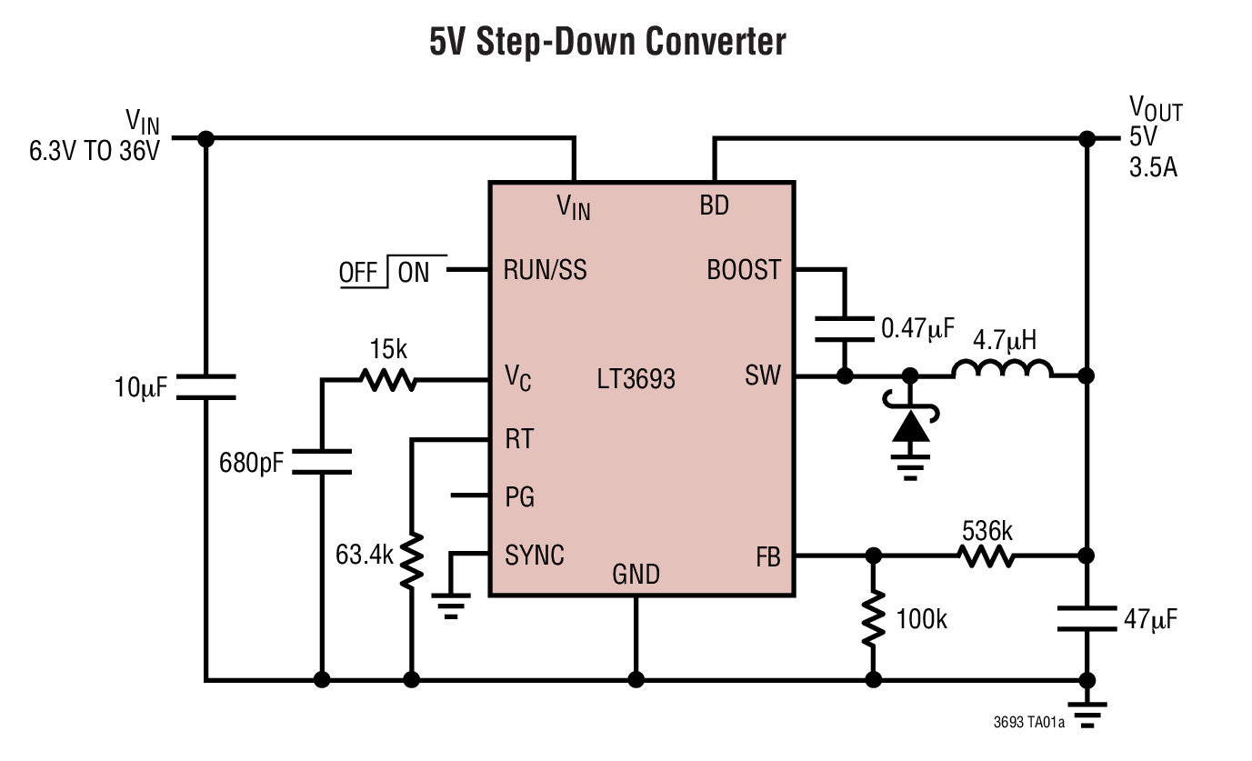
LT3693EMSE Demo Board | 6.3V ≤ VIN ≤ 36V, VOUT = 5V @ 3.5A
Analog Devices Inc.Demonstration circuit 1272 is a monolithic stepdown DC/DC switching regulator featuring LT3693. The demo board is designed for 5V@3.5A output from a 6.3V to 36V input.

LTC3558EUD | Linear USB Battery Charger with Buck and Buck-Boost Regulators
Analog Devices Inc.DC1276B: Demo Board for LTC3558 - Linear USB Battery Charger with Buck and Buck-Boost Regulators

LTC3670EDDB Demo Board | 2.25MHz, Buck Plus Two 150mA LDOs, 2.5V ≤ VIN ≤ 5.5V, VOUT1 = 1.2V @ 400mA, VOUT2 = 2.8V @ 150mA, VOUT3 = 3.3V @ 150mA
Analog Devices Inc.Demo Circuit 1277A is a demo board that features the LTC3670, a triple power supply composed of a 400mA synchronous buck regulator and two 150mA low dropout linear regulators (LDOs). The input supply range is 2.5V to 5.5V and it provides 1.2V @ 400mA, 2.8V @ 150mA and 3.3V @ 150mA. The output regulation of the LDOs is subject to the dropout requirements based on the supply voltage.

DC1278A
Analog Devices Inc.The LTC2351-14 is a 14-bit, 1.5Msps ADC with six simultaneously sampled differential inputs. The device draws only 5.5mA from a single 3V supply, and comes in a tiny 32-pin (5mm ? 5mm) QFN package. A sleep shutdown mode further reduces power consumption to 12?W. The combination of low power and tiny package makes the LTC2351-14 suitable for portable applications.The LTC2351-14 contains six separate differential inputs that are sampled simultaneously on the rising edge of the CONV signal. These six sampled inputs are then converted at a rate of 250ksps per channel.The 83dB common mode rejection allows users to eliminate ground loops and common mode noise by measuring signals differentially from the source.The device converts 0V to 2.5V unipolar inputs differentially, or ?1.25V bipolar inputs also differentially, depending on the state of the BIP pin. Any analog input may swing rail-to-rail as long as the differential input range is maintained.The conversion sequence can be abbreviated to convert fewer than six channels, depending on the logic state of the SEL2, SEL1 and SEL0 inputs.The serial interface sends out the six conversion results in 96 clocks for compatibility with standard serial interfaces. Bits LTC2351-12 12 LTC2351-14 14 Applications Multiphase Power Measurement Multiphase Motor Control Data Acquisition Systems Uninterruptable Power Supplies

DC1280A
Analog Devices Inc.The LT3471 dual switching regulator combines two 42V, 1.3A switches with error amplifiers that can sense to ground providing boost and inverting capability. The low VCESAT bipolar switches enable the device to deliver high current outputs in a small footprint. The LT3471 switches at 1.2MHz, allowing the use of tiny, low cost and low profile inductors and capacitors. High inrush current at start-up is eliminated using the programmable soft-start function, where an external RC sets the current ramp rate. A constant frequency current mode PWM architecture results in low, predictable output noise that is easy to filter.The LT3471 switches are rated at 42V, making the device ideal for boost converters up to ?40V as well as SEPIC and flyback designs. Each channel can generate 5V at up to 630mA from a 3.3V supply, or 5V at 510mA from four alkaline cells in a SEPIC design. The device can be configured as two boosts, a boost and inverter or two inverters.The LT3471 is available in a low profile (0.75mm) 10-lead 3mm ? 3mm DFN package.Applications Organic LED Power Supply Digital Cameras White LED Power Supply Cellular Phones Medical Diagnostic Equipment Local ?5V or ?12V Supply TFT-LCD Bias Supply xDSL Power Supply

LT3496EUFD Demo Circuit | Buck-Boost or Boost Triple Output LED Driver, 8V ≤ VIN ≤ 16V, VLED up to 36V @ 200mA (×3)
Analog Devices Inc.Demonstration circuit 1288 is a Triple Boost or Buck-Boost LED Driver featuring the LT3496EUFD (for evaluating an LT3496 buck mode LED driver, use the demonstration circuit 986). The LT3496 is a triple output DC/DC converter designed to operate as current sources for driving high current LEDs. The board can be configured as either a buck-boost (default) or boost solution. The current for each output is set at 200mA in either mode. The three LEDs are included in the demo board assembly.
The operating power input voltage (PVIN) range is 8V to 16V. The buck-boost circuit can tolerate an input voltage up to 40V when the LED string is on the high side. The part shuts down when the overvoltage threshold is reached. For a typical application with 5 LEDs totaling 16V of LED voltage, the circuit will operate until PVIN reaches 22V if the overvoltage protection is set to 38V.

DC1292A
Analog Devices Inc.The LTC3878 is a synchronous step-down switching DC/DC controller optimized for high switching frequency and fast transient response. The constant on-time valley current mode architecture allows for a wide input range, including very low duty factor operation. No external sense resistor or slope compensation is required. The LTC3878 is pin compatible with the LTC1778 in applications that do not use EXTVCC while offering better efficiency. Consult with the factory to verify compatibility. Operating frequency is set by an external resistor and compensated for variations in VIN to offer excellent line stability. Discontinuous mode operation provides high efficiency during light load conditions. A forced continuous control pin allows the user to reduce noise and RF interference. Safety features include output overvoltage protection and programmable current limit with foldback. Soft-start capability for supply sequencing is accomplished through an external timing capacitor. The current limit is user programmable. The LTC3878 allows operation from 4V to 38V at the input and from 0.8V to 90% VIN at the output. The LTC3878 is available in a small 16-pin narrow SSOP package.Applications Distributed Power Systems Embedded Computing Communications Infrastructure

LT1912EDD | 36V, 2A, 500kHz Step-Down Switching Regulator
Analog Devices Inc.DC1313A: Demo Board for LT1912 36V, 2A, 500kHz Step-Down Switching Regulator.

LT1952EGN-1 Active Reset Demo Board | VIN=18V-72V VOUT=24V @ 5A
Analog Devices Inc.DC1317A-D: Demo Board for LT1952 Single Switch Synchronous Forward Controller.

LTC6802-1 (requires DC590) New Designs Should Use DC1651 or DC1653 | Demo Board
Analog Devices Inc.DC1331D: Demo Board for LTC6802-1 - Multicell Battery Stack Monitor

LTC4269-1 | PoE Powered Device w/48V Isolated Auxiliary, VOUT = 5V, IOUT = 5A
Analog Devices Inc.DC1335B-B: Demo Board for the LTC4269-1 - IEEE 802.3at PD with Synchronous No-Opto Flyback Controller

DC1339A
Analog Devices Inc.The LTC2302/LTC2306 are low noise, 500ksps, 1-/2-channel, 12-bit ADCs with an SPI/MICROWIRE compatible serial interface. These ADCs include a fully differential sample-and-hold circuit to reduce common mode noise. The internal conversion clock allows the external serial output data clock (SCK) to operate at any frequency up to 40MHz. The LTC2302/LTC2306 operate from a single 5V supply and draw just 2.8mA at a sample rate of 500ksps. The auto-shutdown feature reduces the supply current to 14?A at a sample rate of 1ksps. The LTC2302/LTC2306 are packaged in a tiny 10-pin 3mm x 3mm DFN. The low power consumption and small size make the LTC2302/LTC2306 ideal for battery-operated and portable applications, while the 4-wire SPI compatible serial interface makes these ADCs a good match for isolated or remote data acquisition systems.Applications High Speed Data Acquisition Industrial Process Control Motor Control Accelerometer Measurements Battery-Operated Instruments Isolated and/or Remote Data Acquisition

LTC3853EUJ Demo Board | Triple, PolyPhase, 6.5V ≤ VIN ≤ 14V, VOUT1 = 1.8V/15A, VOUT2 = 1.2V/15A, VOUT3 = 2.5V/15A
Analog Devices Inc.Demonstration circuit 1349A is a polyphase 3-output step-down supply with tracking featuring the LTC3853EUJ. The input voltage range is 6.5V to 14V. For applications with narrow, 5V ±0.5V input range, the board has an optional resistor to tie the INTVCC pin to the VIN pin. The demo board provides three 15A outputs, with output voltages of 1.8V, 1.2V and 2.5V.
The main features of the board include rail tracking, an internal 5V linear regulator for bias, RUN pins for each output, two PGOOD signals and a Mode selector that allow the converter to run in CCM, pulse skip or Burst Mode operation. Synchronization to an external clock is also possible through some minor component changes.

DC1350A-B
Analog Devices Inc.The LTC2226H is a 12-bit 25Msps, low power 3V A/D converter designed for digitizing high frequency, wide dynamic range signals. The LTC2226H is perfect for demanding imaging and communications applications with AC performance that includes 71.4dB SNR and 90dB SFDR. DC specs include ?0.3LSB INL (typ), ?0.3LSB DNL (typ) and no missing codes over temperature. The transition noise is a low 0.25LSBRMS. A single 3V supply allows low power operation. A separate output supply allows the outputs to drive 0.5V to 3.6V logic. A single-ended CLK input controls converter operation. An optional clock duty cycle stabilizer allows high performance at full speed for a wide range of clock duty cycles.Applications Automotive Industrial Wireless and Wired Broadband Communication


