Top Manufacturers
Stock

Displaying 2901 - 2920 of 5453

Evaluation Kits from Analog Devices Inc.

LTC3630EMSE Demo Board | 4V ≤ VIN ≤ 65V, VOUT = 1.8V/3.3V/5V/Adjustable @ 500mA

Analog Devices Inc.
Demonstration circuit 2105A is a 500mA output DC/DC power supply. There are two versions: DC2105A-A is a board featuring LTC3630A, with 4V to 76V input range; DC2105A-B is a board featuring LTC3630, with 4V to 65V input range. The LTC3630 operates in a high efficiency Burst Mode® operation and includes internal high and low side switches. The board provides jumper selected output voltages of 1.8V, 3.3V, 5V and an option for additional voltages. LTC3630 has internal soft-start and a provision for increasing soft-start time.

DC2110A

Analog Devices Inc.
The LT8631 is a current mode PWM step-down DC/DC converter with internal synchronous switches that provide current for output loads up to 1A. The wide input range of 3V to 100V makes the LT8631 suitable for regulating power from a wide variety of sources, including automotive and industrial systems and 36V to 72V telecom supplies. Low ripple Burst Mode operation enables high efficiency operation down to very low output currents while keeping the output ripple below 10mVP-P. Resistor programmable 100kHz to 1MHz frequency range and synchronization capability enable optimization between efficiency and external component size. The soft-start feature controls the ramp rate of the output voltage, eliminating input current surge during start-up, while also providing output tracking. A power good flag signals when the output voltage is within ?7.5% of the regulated output. Undervoltage lockout can be programmed using the EN/UV pin. Shutdown mode reduces the total quiescent current to < 5?A. The LT8631 is available in a 20-lead TSSOP package with exposed pad for low thermal resistance and high voltage lead spacing.APPLICATIONS Automotive Supplies Telecom Supplies Distributed Supply Regulation

DC2113A

Analog Devices Inc.
The LTC3649 is a high efficiency 60V, 4A synchronous monolithic step-down regulator. The regulator features a single resistor programmable output voltage, internal compensation and high efficiencies over a wide VOUT range.The step-down regulator operates from an input voltage range of 3.1V to 60V and provides an adjustable rail-to-rail output range from (VIN ? 0.5V) to ground while delivering up to 4A of output current. The switching frequency is also adjusted with an external resistor. A user-selectable mode input is provided to allow the user to trade off ripple noise for efficiency at light loads; Burst Mode operation provides the highest efficiency at light loads, while forced continuous mode provides low output ripple. The MODE/SYNC pin can also be used to allow the user to synchronize the switching frequency to an external clock.The LTC3649 operates with a peak current mode architecture that allows for fast transient response with inherent cycle-to-cycle current limit protection. It also features programmable output current limit, current monitoring and input voltage regulation.Applications Industrial Applications Automotive Applications

LTC4234 Demo Board | 20A Guaranteed SOA Hot Swap Controller

Analog Devices Inc.
Demonstration circuit 2116A features the LTC4233/LTC4234 10A/20A Guaranteed SOA Hot Swap™ Controllers. The LTC4233 and LTC4234 are ideally suited for compact power distribution control in 2.9V to 15V applications for hot board insertion protection, high side power switching, and electronic circuit breaker functions.

LTC3895EFE Demo Board | Synchronous Buck, 14V ≤ VIN ≤ 130V, 150VPK; VOUT = 12V @ 5A

Analog Devices Inc.
Demonstration circuit 2117A is a single output high voltage nonisolated synchronous step-down converter that drives all N-channel MOSFET power stage. It features the LTC3895EFE, a high voltage step-down DC/DC controller housed in a TSSOP-38 package with several pins removed for high voltage spacing.

LTC4040 Demo Board | 5VIN, 2A Single Cell Li-ion/LiFePO4 Buck Battery Charger with 2.5A Boost Backup Power Manager

Analog Devices Inc.
Demonstration circuit 2118B is a combination step-down battery charger and step-up battery backup regulator using the LTC4040 monolithic system power manager. The DC2118B has an input voltage range from 4.8V to 5.5V with overvoltage protection (OVP) to 40V, as limited by the external MOSFET. The input current is monitored to prioritize the load up to the 2.5A threshold before charge current is reduced. Battery Charging As initially configured, DC2118B is programmed for 2A charge current limit when in charge mode. The charge voltage is jumper-selectable in 8 discrete steps from 3.45V to 3.6V for LiFePO4 chemistry or 3.95V to 4.1V for Li-ion chemistry, according to the F2/F1/F0 programming input settings. The charge current limit is adjustable via the PROG pin resistor. End-of-charge status is triggered by current falling below C/8 and indicated by the CHRG LED. The optional NTC input provides temperature fault detection and status indicated by the FAULT LED. Charging can be enabled/disabled with the ENCHG jumper. Battery Backup Following an input power failure, the circuit automatically shifts to battery backup boost mode to regulate the VSYS output rail. The backup mode system output voltage is initially programmed for 5V. The input power failure status is indicated by the PFO LED. If VSYS ever falls below the programmed reset threshold voltage, the RST LED will change states to indicate the need to reset the system and recharge the battery. Backup regulation can be enabled/disabled with the ENBST jumper. For convenience, all LEDs can be disabled with the LED jumper to reduce the quiescent current of the system.

DC2121A

Analog Devices Inc.
The LTM4634 integrates three complete 5A/5A/4A high efficiency switching mode DC/DC converters into one small package. Switching controllers, power FETs, inductors, and most support components are included. Operating over an input voltage range of 4.75V to 28V, the LTM4634 provides three independent output voltages. VOUT1 and VOUT2 are adjustable from 0.8V to 5.5V, while VOUT3 is adjustable from 0.8V to 13.5V. Each output voltage is set by a single external resistor.High switching frequency and a current mode architecture enable a very fast transient response to line and load changes without sacrificing stability. The device supports frequency synchronization, multiphase parallel operation, soft-start and output voltage tracking for supply rail sequencing.Fault protection features include overvoltage protection, overcurrent protection and temperature monitoring. The power module is offered in a space saving, thermally enhanced 15mm ? 15mm ? 5.01mm BGA package. The LTM4634 is available with SnPb (BGA) or RoHS compliant terminal finish.Applications Telecom, Networking and Industrial Equipment High Density Point of Load Voltage Regulation

DC2122A

Analog Devices Inc.
The LTC3859AL is a high performance triple output (buck/buck/boost) synchronous DC/DC switching regulator controller that drives all N-channel power MOSFET stages. Constant frequency current mode architecture allows a phase-lockable switching frequency of up to 850kHz. The LTC3859AL operates from a wide 4.5V to 38V input supply range. When biased from the output of the boost converter or another auxiliary supply, the LTC3859AL can operate from an input supply as low as 2.5V after start-up.The 28?A no-load quiescent current extends operating runtime in battery powered systems. OPTI-LOOP compensation allows the transient response to be optimized over a wide range of output capacitance and ESR values. The LTC3859AL features a precision 0.8V reference for the bucks, 1.2V reference for the boost and a power good output indicator. The PLLIN/MODE pin selects among Burst Mode operation, pulse-skipping mode, or continuous inductor current mode at light loads.Compared to the LTC3859 and the LTC3859A, the LTC3859AL is fully pin-compatible, but with lower Burst Mode operation IQ (28?A with one channel on). Quiescent Current (Burst Mode) Notes LTC3859AL 28?A-One channel on, Buck 38?A-All three channels on Internal clamp on the INTVCC pin LTC3859A 55?A-One channel on, Buck 80?A-All three channels on Internal clamp on the INTVCC pin. For new designs, we recommend LTC3859AL LTC3859 55?A-One channel on, Buck 80?A-All three channels on For new designs, we recommend LTC3859AL Applications Automotive Always-On and Start-Stop Systems Battery Operated Digital Devices Distributed DC Power Systems Multioutput Buck-Boost Applications

DC2131A

Analog Devices Inc.
TheLTC3623 is a high efficiency, monolithic synchronous buck regulator in which the output voltage is programmed with a single external resistor. The accurate internally generated 50?A current source on the ISET pin allows the user to program an output voltage from 0V to 0.5V below VIN. The user can also directly drive the ISET pin with an external voltage supply to program the converter?s VOUT. The VOUT voltage is fed directly back to the error amplifier to be regulated to the ISET voltage. The operating supply voltage range for the SVIN pin is from 15V down to 4V, while the PVIN pin?s voltage range is 15V down to 1.5V, making it suitable for dual Li-Ion batteries and for taking power from a 12V or 5V rail.The operating frequency is programmable from 400KHz to 4MHz with an external RT resistor. Higher switching frequency allows the use of smaller surface mount inductors while lower frequency allows for higher power efficiency. The unique constant-frequency/controlled on-time architecture is ideal for high step-down ratio applications that are operating at high frequency while demanding fast transient response.Applications Tracking Supply or DDR Memory Supply ASIC Substrate Biasing Point-of-Load (POL) Power Supply Portable Instruments, Battery-Powered Equipment Thermo Electric Cooler (TEC) Systems

LTC4020EUHF | High Power Buck-Boost Multi‑Chemistry Battery Charger

Analog Devices Inc.
Demonstration circuit 2134B is a high power buck-boost multi-chemistry battery charger featuring the LTC4020. The board will accept an input voltage between 15V and 55V. The float voltage of the battery output (BAT) is 25.2V, with 6.3A maximum charge current. The converter output (VOUT) has a voltage range of 21V to 28V, with 8A maximum load current. The LTC4020 contains a high efficiency synchronous buck-boost DC/DC controller and uses a proprietary average current mode architecture. The LTC4020 battery charger can provide a constantcurrent/constant-voltage charge algorithm (CC/CV); a four-step, three-stage lead-acid battery-charge profile or constant-current charging (CC). Battery-chemistry type is selected using onboard jumper JP1. The LTC4020 data sheet gives a complete description of the IC operation and application information. The data sheet must be read in conjunction with the quick start guide.

DC2135A

Analog Devices Inc.
The LTC2378-20 is a low noise, low power, high speed 20-bit successive approximation register (SAR) ADC. Operating from a 2.5V supply, the LTC2378-20 has a ?VREF fully differential input range with VREF ranging from 2.5V to 5.1V. The LTC2378-20 consumes only 21mW and achieves ?2ppm INL maximum, no missing codes at 20 bits with 104dB SNR.The LTC2378-20 has a high speed SPI-compatible serial interface that supports 1.8V, 2.5V, 3.3V and 5V logic while also featuring a daisy-chain mode. The fast 1Msps throughput with no cycle latency makes the LTC2378-20 ideally suited for a wide variety of high speed applications. An internal oscillator sets the conversion time, easing external timing considerations. The LTC2378-20 automatically powers down between conversions, leading to reduced power dissipation that scales with the sampling rate.The LTC2378-20 features a unique digital gain compression (DGC) function, which eliminates the driver amplifier?s negative supply while preserving the full resolution of the ADC. When enabled, the ADC performs a digital scaling function that maps zero-scale code from 0V to 0.1 ? VREF and full-scale code from VREF to 0.9 ? VREF. For a typical reference voltage of 5V, the full-scale input range is now 0.5V to 4.5V, which provides adequate headroom for powering the driving amplifier from a single 5.5V supply.Applications Medical Imaging High Speed Data Acquisition Portable or Compact Instrumentation Industrial Process Control Low Power Battery-Operated Instrumentation ATE

LTM4677 Demo Board | µModule PMBus Buck, LTM4677(x3), 4.5V ≤ VIN ≤ 16V, VOUT = 0.5V to 1.8V @ 108A

Analog Devices Inc.
Demonstration circuit 2143A-B is a high efficiency, high density, μModule regulator with 4.5V to 16V input range. The output voltage is adjustable from 0.5V to 1.8V, and it can supply 108A maximum load current. The demo board has three LTM4677 μModule® regulators, and the LTM4677 is a dual 18A or single 36A step-down regulator with PMBus power system management. Please see the LTM4677 data sheet for more detailed information.

LTC5596 Demo Board | 100MHz to 40GHz RMS Power Detector

Analog Devices Inc.
Demonstration circuit 2158A hosts a high accuracy RMS Power Detector featuring the LTC5596 IC. This device is a wide dynamic range RMS RF Power Detector operational from 100MHz to 40GHz. The input dynamic range with 1dB accuracy is up to 35dB depending on frequency. The detector output voltage slope is normally 29mV/dB. The DC2158A Demo Circuit is optimized for wide operational frequency range up to 40GHz with 2.9mm SMK edge mount connector. Input impedance to LTC5596 is internally matched to 50Ω. It is suitable for RMS measurements of high crest factor waveforms up to 12dB peak/average ratio. No external coupling capacitor is necessary if DC voltage at RFIN pin is kept below 1.0V. Contact applications support for more information.

DC2160A

Analog Devices Inc.
The LTC4419 is a dual input monolithic PowerPath? prioritizer with low operating current, that provides backup switchover for keeping critical circuitry alive during brown out and power loss conditions. Unlike diode-OR products, little current is drawn from the inactive supply even if its voltage is greater than the active supply.Internal 2?, current limited PMOS switches provide power path selection from a primary input (V1) or a backup input (V2) to the output. An adjustable voltage monitor set via an external resistive divider provides flexibility in setting the V1 to V2 switchover threshold. When primary input V1 drops, the ADJ monitor input causes OUT to be switched to V2. Fast non-overlap switchover circuitry prevents both reverse and cross conduction while minimizing output droop.The LTC4419 has two auxiliary comparators with open-drain outputs that provide flexible voltage monitoring. The V2ON output indicates if V2 is powering OUT. Freshness seal mode prevents V2 battery discharge during storage or shipment.?Applications Low Power Battery Backup Portable Equipment Point-of-Sale (POS) Equipment

LTM4630EY-1 Demo Board | 4 Paralleled Buck µModules, 4.5V ≤ VIN ≤ 15V, VOUT = 0.9V to 1.8V @ 140A

Analog Devices Inc.
Demonstration Circuit 2164A-C features a PolyPhase® design using four paralleled LTM4630EY-1's (A-grade), the high efficiency, high density, dual 18A, switch mode step-down power module regulator. The input voltage is from 4.5V to 15V. The output voltage is jumper selectable and can be set to 0.9V, 1.0V, 1.2V, 1.5V or 1.8V. DC2164A-C can deliver nominal 140A output current. As explained in the data sheet, output current derating is necessary for certain VIN, VOUT, and thermal conditions. The LTM4630-1A on the DC2164A-C always operate in continuous conduction mode. The switching frequency can be programmed through a resistor or can be synchronized to an external clock signal. The board allows the user to program how its output voltage ramps up and down through the TRACK pin.

DC2177A-B

Analog Devices Inc.
The LT3062 is a micropower, low dropout (LDO) linear regulator that operates over a 1.6V to 45V supply range and is available in a series of fixed output and adjustable versions. The device supplies 200mA of output current with a typical dropout voltage of 300mV. A single external capacitor provides programmable low noise reference performance and output soft-start functionality. The LT3062?s quiescent current is merely 45?A and provides fast transient response with a minimum 3.3?F output capacitor. In shutdown, quiescent current is less than 1?A and the reference soft start capacitor is reset.The LT3062 optimizes stability and transient response with low ESR, ceramic output capacitors. The LT3062 does not require the addition of ESR as is common with other regulators.Internal protection circuitry includes reverse-battery protection, reverse-output protection, reverse-current protection, current limit with foldback and thermal shutdown.The LT3062 is available in fixed output voltages of 3.3V and 5V, and as an adjustable device with an output voltage range from the 600mV reference up to 40V. The LT3062 is offered in the thermally enhanced 8-lead 2mm ? 3mm DFN and MSOP packages.Applications Battery Powered Systems Automotive Power Supplies Industrial Power Supplies Avionic Power Supplies Portable Instruments

LTC2645 Demo Board | Quad 12-/10-/8-BIT PWM to VOUT DACs (requires DC2026)

Analog Devices Inc.
Demonstration circuit 2197A features the LTC2645, Quad 12-/10-/8-Bit PWM to VOUT DACs with 10ppm/°C reference in a tiny 4.9mm × 4mm 16-lead MSOP package. DC2197A-A is populated with the 2.5V, 12-bit version of the LTC2645.

DC2215A

Analog Devices Inc.
The LTC3126 is a high efficiency synchronous buck converter with an internal no-loss PowerPath? supporting seamless operation from two separate input power sources. Pin selectable ideal diode-OR and priority input modes with user programmable undervoltage lockout thresholds provide full control over the transition between the input power sources. The fast, automatic switchover provided by the internal PowerPath eliminates the need for hold-up capacitors and minimizes disturbances on the output rail. An active input channel indicator and independent input and output power good signals provide complete feedback of the power system status.A wide 2.4V to 42V input voltage range, 2.5A output current capability and 2?A Burst Mode operation quiescent current facilitate use of the LTC3126 with a wide variety of power sources including supercapacitors, automotive batteries, unregulated wall adapters and single to multicell stacks of most battery chemistries. Additional features include 1?A current in shutdown, internal soft-start and thermal protection. The LTC3126 is available in thermally enhanced 28-lead 4mm ? 5mm QFN and 28-lead TSSOP packages.Applications Portable Industrial/Communications Test Equipment Battery and Supercapacitor Backup Power Automotive Power with Battery Backup Uninterruptible Power Supplies

DC2229A-B

Analog Devices Inc.
The LTC3877 is a VID-programmable, constant frequency current mode step-down controller using an advanced and proprietary architecture. This new architecture enhances the signal-to-noise ratio of the current sense signal, allowing the use of very low DC resistance power inductors to maximize efficiency in high current applications. This feature also dramatically reduces the current sensing error, so that current sharing is greatly improved in multi-phase low DCR applications. In addition, the controller achieves a minimum on-time of just 40ns, permitting the use of high switching frequency at high step-down ratios.The LTC3877 features dual high speed remote sense differential amplifiers, programmable current sense limits and DCR temperature compensation to limit the maximum output current precisely over temperature. The LTC3877 also features a precise 0.6V reference with guaranteed accuracy of ?0.5%. The LTC3877 is available in a low profile 44-lead 7mm ? 7mm QFN package.Applications FPGAs and Processor Power Servers and Computing

DC2235A

Analog Devices Inc.
The LTC3265 is a low noise dual polarity output power supply including a boost charge pump, an inverting charge pump and two low noise positive and negative LDO post regulators. The boost charge pump powers the positive LDO post regulator while the inverting charge pump powers the negative LDO regulator. Each LDO can provide up to 50mA of output current. The LDO output voltages can be adjusted using external resistor dividers.The charge pumps employ low quiescent current Burst Mode operation or low noise constant frequency mode. During Burst Mode operation, the boost charge pump regulates its output (VOUT +) to 0.94 ? 2 ? VIN_P while the inverting charge pump regulates its output (VOUT ?) to ?0.94 ? VIN_N. In Burst Mode operation the LTC3265 draws only 135?A of quiescent current with both LDOs on. In constant frequency mode, the boost and inverting charge pumps produce outputs equal to 2 ? VIN_P and ?VIN_N respectively and operate at a fixed 500kHz or to a programmed value between 50kHz to 500kHz using an external resistor. The LTC3265 is available in low profile 3mm ? 5mm ? 0.75mm 18-lead DFN and thermally enhanced 20-lead TSSOP packages.Applications Low Noise Bipolar/Inverting Supplies Industrial/Instrumentation Low Noise Bias Generators

Displaying 2901 - 2920 of 5453

Latest Parts

IN STOCK 13664
Buy

ASX00049

Arduino

$32.41 - $65.06

IN STOCK 2847
Buy

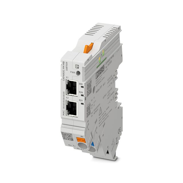
1687559

Phoenix Contact Ltd

[no prices available]

IN STOCK 2
Buy

Reference Designs

RD006

Wurth Elektronik

RD006 - 3 W Dual-output isolated auxiliary supply for communication interfaces and measurement systems

CN0583

Analog Devices Inc.

Multistandard Micropower Verified Smoke Detection System-on-Module

Technical Resources

EVALUATION KITS

EVAL-AD7124-8SDZ

Analog Devices Inc.

$0.00 - * $79.60

IN STOCK 792
Buy
View All