
109293-HMC535LP4
Analog Devices Inc.The HMC535LP4(E) is a GaAs InGaP Heterojunction Bipolar Transistor (HBT) MMIC PLO. The PLO?s phase noise performance is excellent over temperature, shock, and process due to the oscillator?s monolithic structure. Power output is +9 dBm typical from a +5V supply voltage.All functions (VCO, Op-Amp, PFD, Prescaler) are fully integrated while providing allowances for off-chip customer specific loop components. The PLO MMIC accepts a single-ended or a differential reference oscillator input signal in the range of 230 to 240 MHz, and a digital Lock Detector (LD) output is provided to confirm the status of the loop. The phase-locked oscillator is packaged in a leadless QFN 4?4 mm surface mount package.APPLICATIONS VSAT Radio? Point-to-Point & Point-to-Multi-Point Radio? Test Equipment & Industrial Controls? Military End-Use

109994-HMC453QS16G
Analog Devices Inc.The HMC453QS16G(E) is a high dynamic range GaAs InGaP Heterojunction Bipolar Transistor (HBT) 1.6 watt MMIC power amplifier operating between 0.4 and 2.2 GHz. Packaged in a miniature 16 lead QSOP plastic package, the amplifier gain is typically 21.5 dB at 0.4 GHz and 8 dB at 2.1 GHz. Utilizing a minimum number of external components and a single +5V supply, the amplifier output IP3 can be optimized to +47 dBm at 0.4 GHz or +51 dBm at 2.1 GHz. The power control (VPD) can be used for full power down or RF output power/current control. The high output IP3 and PAE make the HMC453QS16G(E) ideal power amplifier for Cellular/ PCS/3G, WLL, ISM and Fixed Wireless applications.Applications GSM, GPRS & EDGE? CDMA & W-CDMA? CATV/Cable Modem? Fixed Wireless & WLL

110227-HMC507LP5
Analog Devices Inc.The HMC507LP5(E) is a GaAs InGaP Heterojunction Bipolar Transistor (HBT) MMIC VCO. The HMC507LP5(E) integrates resonators, negative resistance devices, varactor diodes and feature a half frequency output. The VCO?s phase noise performance is excellent over temperature, shock, and process due to the oscillator?s monolithic structure. Power output is +13.5 dBm typical from a +5V supply. The voltage controlled oscillator is packaged in a leadless QFN 5x5 mm surface mount package, and requires no external matching components.APPLICATIONS VSAT Radio Point to Point/Multi-Point Radio? Test Equipment & Industrial Controls? Military End-Use

110227-HMC509LP5
Analog Devices Inc.The HMC509LP5(E) is a GaAs InGaP Heterojunction Bipolar Transistor (HBT) MMIC VCOs. The HMC509LP5(E) integrates resonators, negative resistance devices, varactor diodes and feature a half frequency output. The VCO?s phase noise performance is excellent over temperature, shock, and process due to the oscillator?s monolithic structure. Power output is +13 dBm typical from a +5V supply. The voltage controlled oscillator is packaged in a leadless QFN 5x5 mm surface mount package, and requires no external matching components.APPLICATIONS VSAT Radio? Point-to-Point/Multi-Point Radio? Test Equipment & Industrial Controls? Military End-Use

110227-HMC515LP5
Analog Devices Inc.The HMC515LP5(E) is a GaAs InGaP Heterojunction Bipolar Transistor (HBT) MMIC VCO. The HMC515LP5(E) integrates resonators, negative resistance devices, varactor diodes and feature half frequency and divide-by-4 outputs. The VCO?s phase noise performance is excellent over temperature, shock, and process due to the oscillator?s monolithic structure. Power output is +10 dBm typical from a +5V supply voltage. The prescaler function can be disabled to conserve current if not required. The voltage controlled oscillator is packaged in a leadless QFN 5x5 mm surface mount package, and requires no external matching components.APPLICATIONS VSAT Radio? Point-to-Point/Multi-Point Radio? Test Equipment & Industrial Controls? Military End-Use

110227-HMC534LP5
Analog Devices Inc.The HMC534LP5(E) is a GaAs InGaP Heterojunction Bipolar Transistor (HBT) MMIC VCO. The HMC534LP5(E) integrates resonators, negative resistance devices, varactor diodes and feature half frequency and divide-by-4 outputs. The VCO?s phase noise performance is excellent over temperature, shock, and process due to the oscillator?s monolithic structure. Power output is +11 dBm typical from a +5V supply voltage. The prescaler and RF/2 functions can be disabled to conserve current if not required. The voltage controlled oscillator is packaged in a leadless QFN 5x5 mm surface mount package, and requires no external matching components.APPLICATIONS Point-to-Point/Multi-point Radio Test Equipment & Industrial Controls SATCOM Military End-Use

110227-HMC632LP5
Analog Devices Inc.The HMC632LP5(E) is a GaAs InGaP Heterojunction Bipolar Transistor (HBT) MMIC VCO. The HMC632LP5(E) integrates resonators, negative resistance devices, varactor diodes and features half frequency and divide-by-4 outputs. The VCO?s phase noise performance is excellent over temperature, shock, and process due to the oscillator?s monolithic structure. Power output is +9 dBm typical from a +5V supply voltage. The prescaler and RF/2 functions can be disabled to conserve current if not required. The voltage controlled oscillator is packaged in a leadless QFN 5x5 mm surface mount package, and requires no external matching components.APPLICATIONS Point to Point/Multipoint Radio Test Equipment & Industrial Controls SATCOM Military End-Use

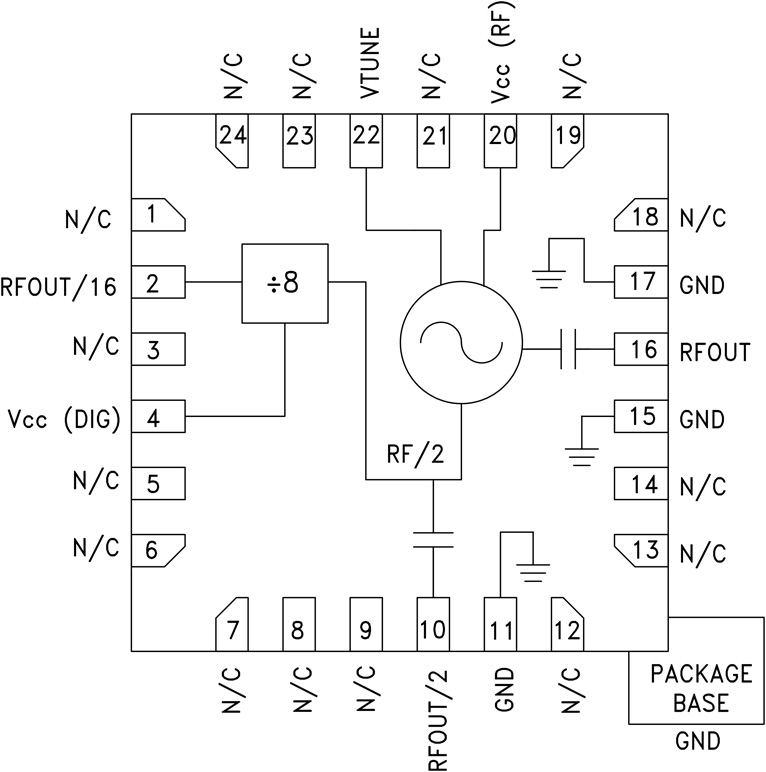
110227-HMC734LP5
Analog Devices Inc.The HMC734 is a GaAs InGaP Heterojunction Bipolar Transistor (HBT) MMIC VCO. The HMC734 integrates a resonator, negative resistance device, varactor diode and features a divide-by-4 frequency output. The VCO's phase noise performance is excellent over temperature, shock, and process due to the oscillator's monolithic structure. Power output is +18 dBm typical from a +5V supply voltage. The prescaler function can be disabled to conserve current if not required. The voltage controlled oscillator is packaged in a leadless QFN 5?5 mm surface mount package, and requires no external matching components.APPLICATIONS Point-to-Multi-Point Radios Test Equipment & Industrial Controls SATCOM Military End-Use
112261-HMC738LP4
Analog Devices Inc.The HMC738 is a GaAs InGaP Heterojunction Bipolar Transistor (HBT) MMIC VCO. The HMC738 integrates a resonator, negative resistance device, varactor diode and divide-by-16 prescaler. The VCOs phase noise performance is excellent over temperature, shock, and process due to the oscillator's monolithic structure. Power output is +9 dBm typical from a 5V supply voltage. The voltage controlled oscillator is packaged in a low cost leadless QFN 4x4 mm surface mount package.APPLICATIONS Point-to-Point Radios Point-to-Multi-Point Radios/LMDS VSAT

112763-HMC608LC4
Analog Devices Inc.The HMC608LC4 is a high dynamic range GaAspHEMT MMIC Medium Power Amplifier housed in aleadless ?Pb free? SMT package. The amplifier hastwo modes of operation: high gain mode (Vpd pinshorted to ground); and low gain mode (Vpd pin leftopen). The electrical specifications in the table beloware shown for the amplifier operating in high gainmode. Operating from 9.5 to 11.5 GHz, the amplifierprovides 29.5 dB of gain, +27.5 dBm of saturatedpower and 23% PAE from a +5V supply voltage.Noise figure is 6 dB while output IP3 is +33 dBm. TheRF I/Os are DC blocked and matched to 50 Ohmsfor ease of use. The HMC608LC4 eliminates theneed for wire bonding, allowing use of surface mountmanufacturing techniques.Applications? Point-to-Point Radios? Point-to-Multi-Point Radios? Military End-Use

113589-HMC3653LP3B
Analog Devices Inc.The HMC3653LP 3BE is a HBT Gain Block MMI Camplifier covering 7 GHz to 15 GHz and packagedin a 3x3 mm plastic QFN SM T package. This versatileamplifier can be used as a cascadable IF or RF gainstage in 50 Ohm applications. The HMC3653LP 3BEdelivers 15 dB gain, and +15 dBm output P1dB withonly 4 dB noise figure.Applications Point-to-Point Radios Point-to-Multipoint Radios VSAT LO Driver for HMC Mixers Military EW & ECM

114399-HMC542BLP4
Analog Devices Inc.The HMC542BLP4E is a broadband 6-bit GaAs IC digital attenuator with a CMOS compatible serial to parallel driver in low cost leadless surface mount package. This serial control digital attenuator incorporates off chip AC ground capacitors for near DC operation, making it suitable for a wide variety of RF and IF applications. Covering DC to 4 GHz, the insertion loss is 1.7 dB and the attenuator bit values are 0.5 (LSB), 1, 2, 4, 8, and 16 dB for a total attenuation of 31.5 dB. Attenuation accuracy is excellent at ?0.25 dB typical step error with an IIP3 of +50 dBm. Six bit serial control words are used to select each attenuation state. A single VCC bias of +5V is required.APPLICATIONS Cellular/PCS/3G Infrastructure ISM, MMDS, WLAN, WiMAX, & WiBro Microwave Radio & VSAT Test Equipment and Sensors

118040-HMC311SC70
Analog Devices Inc.The HMC311SC70(E) is a GaAs InGaP Heterojunction Bipolar Transistor (HBT) Gain Block MMIC SMT DC to 8 GHz amplifier. Packaged in an industry standard SC70, the amplifier can be used as either a cascadable 50 Ohm gain stage or to drive the LO port of HMC mixers with up to +15 dBm output power. The HMC311SC70(E) offers 15 dB of gain and an output IP3 of +30 dBm while requiring only 54 mA from a +5V supply. The Darlington topology results in reduced sensitivity to normal process variations, and yields excellent gain stability over temperature while requiring a minimal number of external bias components.Applications Cellular / PCS / 3G WiBro / WiMAX / 4G Fixed Wireless & WLAN CATV, Cable Modem & DBS Microwave Radio & Test Equipment

118097-HMC646LP2
Analog Devices Inc.The HMC646LP2(E) is an SPDT switch in a leadless DFN surface mount plastic package for use in transmit / receive and LNA protection applications which require very low distortion and high power handling of up to 40 watts with less than 10% duty cycle. This robust switch can control signals from 100 - 2100 MHz* and is ideal for TD-SCDMA / 3G repeaters, PMR, automotive telematics, and satellite subscriber terminal applications. The design provides exceptional P0.1 dB of +46 dBm and +74 dBm IIP3 on the Transmit (Tx) port. The failsafe topology provides a low loss path from Tx to RFC, when no DC power is available.APPLICATIONS LNA Protection & T/R Switching TD-SCDMA / 3G Infrastructure Satellite Subscriber Terminals Private Mobile Radio & Public Safety Handsets Automotive Telematics
118099-HMC646LP2
Analog Devices Inc.The HMC646LP2(E) is an SPDT switch in a leadless DFN surface mount plastic package for use in transmit / receive and LNA protection applications which require very low distortion and high power handling of up to 40 watts with less than 10% duty cycle. This robust switch can control signals from 100 - 2100 MHz* and is ideal for TD-SCDMA / 3G repeaters, PMR, automotive telematics, and satellite subscriber terminal applications. The design provides exceptional P0.1 dB of +46 dBm and +74 dBm IIP3 on the Transmit (Tx) port. The failsafe topology provides a low loss path from Tx to RFC, when no DC power is available.APPLICATIONS LNA Protection & T/R Switching TD-SCDMA / 3G Infrastructure Satellite Subscriber Terminals Private Mobile Radio & Public Safety Handsets Automotive Telematics

118329-HMC627ALP5
Analog Devices Inc.The HMC627ALP5E is a digitally controlled variable gain amplifier which operates from 50 MHz to 1 GHz, and can be programmed to provide anywhere from 11.5 dB attenuation, to 20 dB of gain, in 0.5 dB steps. The HMC627ALP5E delivers noise figure of 4.3 dB in its maximum gain state, with output IP3 of up to +36 dBm in any state. The dual mode gain control interface accepts either three wire serial input or 6 bit parallel word. The HMC627ALP5E also features a user selectable power up state and a serial output for cascading other Hittite serially controlled components. The HMC627ALP5E is housed in a RoHS compliant 5x5 mm QFN leadless package, and requires no external matching components.Applications Cellular / 3G Infrastructure WiBro / WiMAX / 4G Microwave Radio & VSAT Test Equipment & Sensors IF & RF Applications
119171-HMC681ALP5
Analog Devices Inc.The HMC681ALP5E is a digitally controlled variable gain amplifier which operates from DC to 1 GHz, and can be programmed to provide anywhere from 13.5 dB, to 45 dB of gain, in 0.5 dB steps. The HMC681ALP5E delivers noise figure of 2.8 dB in its maximum gain state, with output IP3 of up to +36 dBm in any state. This serially controlled digital VGA incorporates off chip AC ground capacitors for near DC operation, making it suitable for a wide variety of RF and IF applications. The HMC681ALP5E is housed in a RoHS compliant 5x5 mm QFN leadless package, and provides the user with a highly integrated solution. This functionality is also available with parallel control as the HMC626ALP5E.Applications IF & RF Applications Cellular/3G Infrastructure WiBro / WiMAX / 4G Microwave Radio & VSAT Test Equipment and Sensors
119197-HMC655LP2E
Analog Devices Inc.The HMC652LP2E / 653LP2E / 654LP2E / 655LP2E are a line of wideband fixed value SMT 50 Ohm matched attenuators which offer attenuation levels of 2, 3, 4 and 6 dB respectively. These passive attenuators are ideal for military, test equipment, and other wideband applications where extremely flat attenuation, and excellent VSWR vs. frequency are required.These wideband attenuators handle up to +25 dBm of input power, and are compatible with high volume surface mount manufacturing techniques.APPLICATIONS Fiber Optics Microwave Radio Military & Space Test & Measurement Scientific Instruments RF/Microwave Circuit Prototyping

119394-HMC636ST89
Analog Devices Inc.The HMC636ST89(E) is a GaAs PHEMT, High Linearity, Low Noise, Wideband Gain Block Amplifier covering 0.2 to 4.0 GHz. Packaged in an industry standard SOT89, the amplifier can be used as either a cascadable 50 Ohm gain stage, a PA Pre-Driver, a Low Noise Amplifier, or a Gain Block with up to +23 dBm output power. This versatile Gain Block Amplifier is powered from a single +5V supply and requires no external matching components. The internally matched topology makes this amplifier compatible with virtually any PCB material or thickness.Applications Cellular / PCS / 3G WiMAX, WiBro, & Fixed Wireless CATV & Cable Modem Microwave Radio?

119935-HMC685LP4
Analog Devices Inc.The HMC685LP4(E) is a high dynamic range passive MMIC mixer with integrated LO amplifier in a 4x4 SMT QFN package covering 1.7 to 2.2 GHz. Excellent input IP3 performance of +32 dBm for down conversion is provided for 3G & 4G GSM/CDMA applications at an LO drive of 0 dBm. With an input 1 dB compression of +27 dBm, the RF port will accept a wide range of input signal levels. Conversion loss is 8 dB typical. The DC to 500 MHz IF frequency response will satisfy GSM/CDMA transmit or receive frequency plans. The HMC685LP4(E) is pin for pin compatible with the HMC684LP4(E) which is a 700 - 1000 MHz mixer with LO amplifier.APPLICATIONS Cellular/3G & LTE/WiMAX/4G Basestations & Repeaters GSM, CDMA & OFDM Transmitters and Receivers


