DC1147A-D
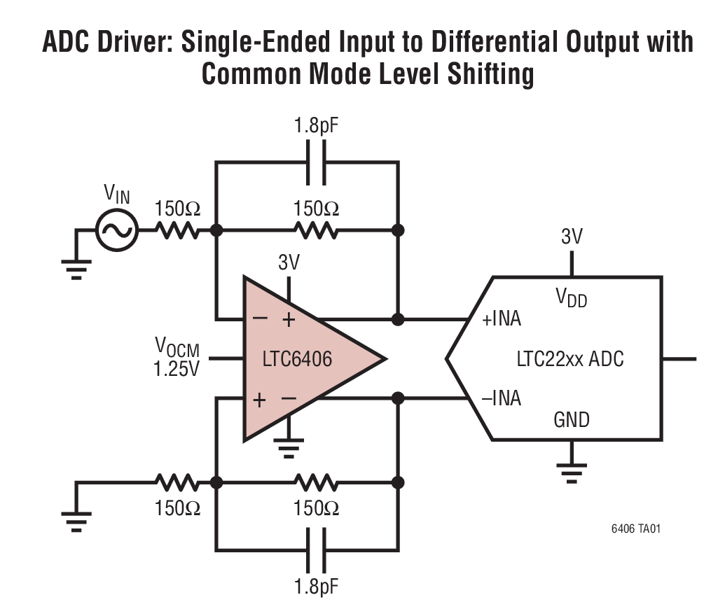
Analog Devices Inc.The LTC6406 is a very low noise, low distortion, fully differential input/output amplifier optimized for 3V, single supply operation. The LTC6406 input common mode range is rail-to-rail, while the output common mode voltage is independently adjustable by applying a voltage on the VOCM pin. This makes the LTC6406 ideal for level shifting signals with a wide common mode range for driving 12-bit to 16-bit single supply, differential input ADCs. A 3GHz gain-bandwidth product results in 70dB linearity for 50MHz input signals. The LTC6406 is unity gain stable and the closed-loop bandwidth extends from DC to 800MHz. The output voltage swing extends from near-ground to 2V, to be compatible with a wide range of ADC converter input requirements. The LTC6406 draws only 18mA, and has a hardware shutdown feature which reduces current consumption to 300?A. The LTC6406 is available in a compact 3mm x 3mm 16-pin leadless QFN package as well as an 8-lead MSOP package, and operates over a ?40?C to 85?C temperature range. Applications Differential Input ADC Driver Single-Ended to Differential Conversion Level-Shifting Ground-Referenced Signals Level-Shifting VCC-Referenced Signals High-Linearity Direct Conversion Receivers

LT3680EMSE Demo Board | 6.3V ≤ VIN ≤ 36V, VOUT = 5V @ 3.5A
Analog Devices Inc.Demonstration circuit 1149 is a monolithic step-down DC/DC switching regulator featuring LT3680. The LT3680 can be synchronized over a 250 kHz to 2 MHz range. The demo board is designed for 5V/3.5A output from a 6.3V to 36V input.

LT3009EDC Demo Board | Micropower Low Dropout Linear Regulator, 1.6V ≤ VIN ≤ 20V, VOUT = 1.2V/1.5V/1.8V/2.0V/2.5V/3.3V/5V/Adjustable @ 20mA
Analog Devices Inc.Demonstration circuit 1156A is an ultralow quiescent current and low dropout voltage linear regulator featuring the 20mA output current LT3009 in the which comes in the 2mm × 2mm DFN package. The DC1156A has an input voltage range from 1.6V to 20V and has jumper-selectable output voltages of 1.2V, 1.5V, 1.8V, 2.0V, 2.5V, 3.3V, 5V or a user-defined value.
With the 3µA quiescent current of the LT3009, the DC1156A is ideal for supplying power to low current battery-powered systems, keep-alive power supply and remote monitoring utility meters and hotel door locks.

DC1157A
Analog Devices Inc.The LT3510 is a dual current mode PWM step-down DC/DC converter with two internal 2.5A switches. Independent input voltage, feedback, soft-start and power good pins for each channel simplify complex power supply tracking/sequencing requirements.Both converters are synchronized to either a common external clock input or a resistor programmable ?xed 250kHz to 1.5MHz internal oscillator. At all frequencies, a 180? phase relationship between channels is maintained, reducing voltage ripple and component size. Programmable frequency allows for optimization between efficiency and external component size.Minimum input-to-output voltage ratios are improved by allowing the switch to stay on through multiple clock cycles, only switching off when the boost capacitor needs recharging, resulting in ~95% maximum duty cycle.Each output can be independently disabled using its own soft-start pin, or by using the SHDN pin the entire part can be placed in a low quiescent current shutdown mode.The LT3510 is available in a 20-lead TSSOP package with exposed leadframe for low thermal resistance.Applications DSP Power Supplies Disc Drives DSL/Cable Modems Wall Transformer Regulation Distributed Power Regulation PCI Cards

DC115A-B
Analog Devices Inc.The LTC1451/LTC1452/LTC1453 are complete single supply, rail-to-rail voltage output 12-bit digital-to-analog converters (DACs) in an SO-8 package. They include an output buffer amplifier and an easy-to-use 3-wire cascadable serial interface. The LTC1451 has an onboard reference of 2.048V and a full-scale output of 4.095V. It operates from a single 4.5V to 5.5V supply. The LTC1452 is a multiplying DAC with a full-scale output of twice the reference input voltage. It operates from a single supply of 2.7V to 5.5V. The LTC1453 has an onboard 1.22V reference and a full-scale output of 2.5V. It operates from a single supply of 2.7V to 5.5V.The low power supply current makes the LTC1451 family ideal for battery-powered applications. The space saving 8-pin SO package and operation with no external components provide the smallest 12-bit DAC system available.Applications Digital Calibration Industrial Process Control Automatic Test Equipment Cellular Telephones

LTC3212EDDB | RGB LED Driver and Charge Pump, 2.7V ≤ VIN ≤ 5.5V, VLED up to 5V @ 25mA (×3) (DC590 Requires)
Analog Devices Inc.Demonstration circuit 1187 is an RGB LED Driver and Charge Pump featuring the LTC3212. The LTC3212 is a low noise boost charge pump capable of driving three LEDs at up to 25mA each. The charge pump operates in either 1x or 2x mode, with automatic mode switching. Individual current sources allow each LED to be turned on individually, in combination with the other LEDs, or in white mode using a single wire interface. The demo board input voltage range is 2.7V to 5.5V. White mode optimizes the red, green, and blue current settings to provide the best white color. LED currents are regulated using internal low dropout current sources. Automatic mode switching optimizes efficiency by switching modes only when a dropout is detected.

LTC2366 Demo Board | 12-Bit, 3Msps SAR ADC (Requires DC590B for DC Apps, DC890B for AC Apps)
Analog Devices Inc.DC1190A-A: Demo Board for the LTC2366 3Msps, 12-Bit Serial ADCs in TSOT-23

LTM8020 Demo Board | µModule DC/DC Regulator, 4.5V ≤ VIN ≤ 36V, VOUT = 3.3V @ 200mA
Analog Devices Inc.Demonstration circuit DC1194A features the LTM8020, a 200mA DC/DC step-down μModule® regulator. The board is preset to deliver a 3.3V output at up to 200mA load current from an input voltage from 4.5V up to 36V. The output voltage may be modified by simply changing one resistor.

DC1195A
Analog Devices Inc.The LTM8023 is a complete 2A, DC/DC step-down power supply. Included in the package are the switching controller, power switches, inductor, and all support components. Operating over an input voltage range of 3.6V to 36V, the LTM8023 supports an output voltage range of 0.8V to 10V, and a switching frequency range of 200kHz to 2.4MHz, each set by a single resistor. Only the bulk input and output filter capacitors are needed to finish the design.The low profile package enables utilization of unused space on the bottom of PC boards for high density point of load regulation.The LTM8023 is packaged in a thermally enhanced, compact and low profile over-molded land grid array (LGA) and ball grid array (BGA) packages suitable for automated assembly by standard surface mount equipment. The LTM8023 is available with SnPb (BGA) or RoHS compliant terminal finish.Applications Automotive Battery Regulation Power for Portable Products Distributed Supply Regulation Industrial Supplies Wall Transformer Regulation

DC1199A
Analog Devices Inc. The LT3595 is a high performance LED Driver designed to drive sixteen independent channels of up to 10 LEDs at currents up to 50mA. Series connection of the LEDs provides identical LED currents resulting in uniform brightness. Power switches, Schottky diodes, and compensation components are all internal, providing a small converter footprint and lower component cost. The high 2MHz switching frequency permits the use of tiny, low pro? le inductors and capacitors. A fixed frequency, current mode architecture results in stable operation over a wide range of supply and output voltage. A single external resistor sets the LED current for all sixteen channels, and dimming is then controlled for each channel by pulse width modulating the individual PWM pins. Relative current matching among the sixteen drivers is 8% and the PWM dimming range is 5000:1. The part is available in a 5mm x 9mm x 0.75mm 56-pin QFN package. Applications LED Video Billboards LCD Televisions Stadium and Advertising Displays

LTC4357 Positive High Voltage Ideal Diode Controller
Analog Devices Inc.DC1203A: Demo Board for LTC4357 Positive High Voltage Ideal Diode Controller.
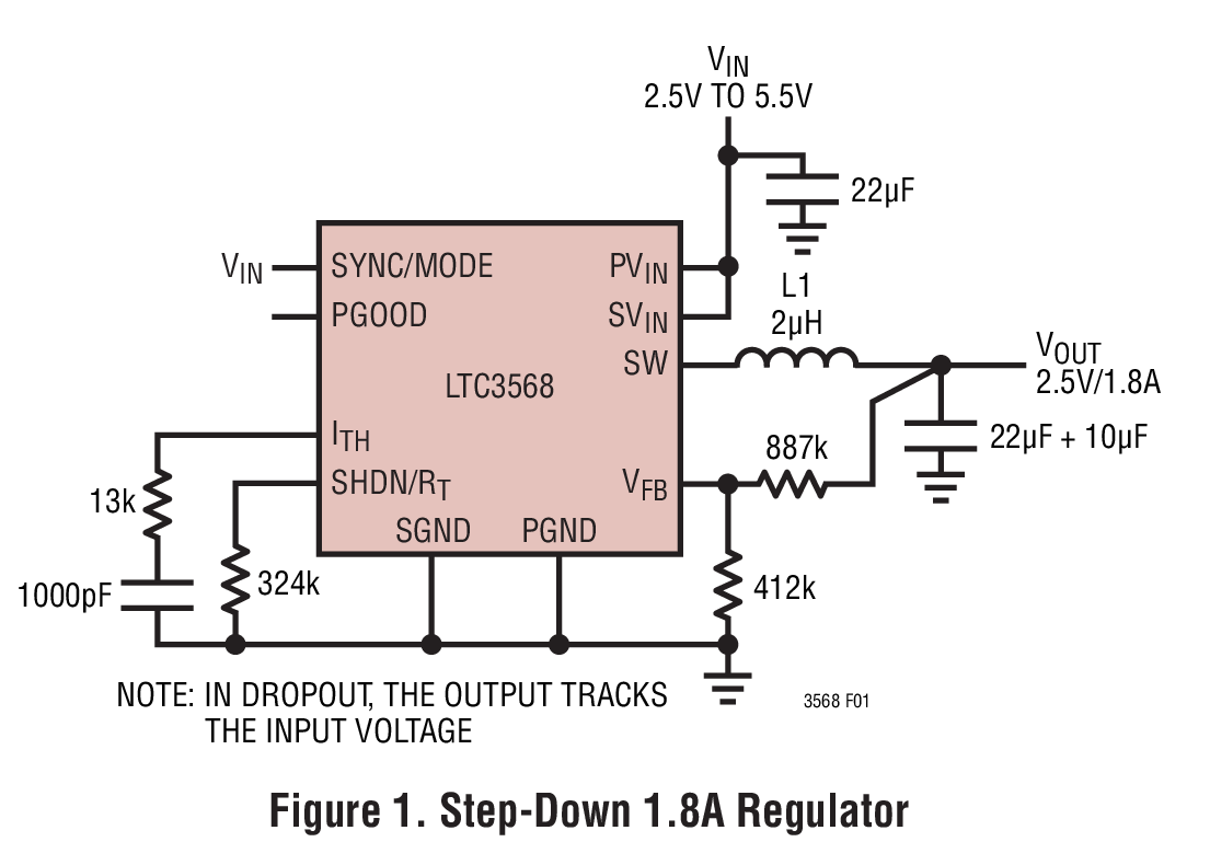
LTC3568EDD Demo Board | 2.25V ≤ VIN ≤ 5.5V, VOUT = 1.2V/1.5V/1.8V at 1.8A
Analog Devices Inc.Demonstration circuit 1206 is a step-down converter, using the LTC3568 monolithic synchronous buck regulator. The DC1206 has an input voltage range of 2.25V to 5.5V, and is capable of delivering up to 1.8A of output current at a minimum input voltage of 2.25V. The output voltage of the DC1206 can be set as low as 0.8V, the reference voltage of the LTC3568. At low load currents, the DC1206 can operate in either noise sensitive applications, due to the capability of the LTC3568 to operate in pulse-skipping mode, or in high efficiency applications, because the LTC3568 can also operate in Burst-Mode®. During Burst-Mode® operation, the output ripple voltage is still low – less than 30 mV – due to the improvements made in the design of the LTC3568.

LTC4151 Demo Board | 80V High Side Power Monitor, Requires DC2026
Analog Devices Inc.Demonstration circuit 1208A features the LTC4151 high side power monitor that accepts input voltages from 7V to 80V. In default operation mode, the onboard 12-bit ADC continuously measures high side current, input voltage and an external voltage. Data is reported through the I2C interface when polled by a host. The monitors can also perform on-demand measurement in a snapshot mode. The LTC4151 features a dedicated shutdown pin to reduce power consumption.

LT3495BEDDB Demo Board | Micropower 3-6VIN to 15VOUT at 75mA
Analog Devices Inc.Demonstration circuit 1219A-A, A-B, A-C and A-D are micropower low noise boost converters with output disconnect featuring the four different LT3495 versions: LT3495 (0.65A switch current, switching frequency above audible range), LT3495B (0.65A switch current), LT3495-1 (0.35 switch current, switching frequency above audible range) and LT3495B-1 (0.35A switch current). All versions convert a 3V-6V source to 15V. The A-A and A-B versions supply 75mA at 3VIN, while the A-C and A-D supply 36mA.
All versions feature a low noise control scheme, integrated output disconnect function, dimming control and a single output sense resistor.
LT3495BEDDB-1 Demo Board | 3-6VIN to 15VOUT at 36mA
Analog Devices Inc.Demonstration circuit 1219A-A, A-B, A-C and A-D are micropower low noise boost converters with output disconnect featuring the four different LT3495 versions: LT3495 (0.65A switch current, switching frequency above audible range), LT3495B (0.65A switch current), LT3495-1 (0.35 switch current, switching frequency above audible range) and LT3495B-1 (0.35A switch current). All versions convert a 3V-6V source to 15V. The A-A and A-B versions supply 75mA at 3VIN, while the A-C and A-D supply 36mA.
All versions feature a low noise control scheme, integrated output disconnect function, dimming control and a single output sense resistor.

LT3682EDD Demo Board | 6.9V ≤ VIN ≤ 36V (60V Transients), VOUT = 5V @ 2A
Analog Devices Inc.Demonstration circuit 1222 is a monolithic stepdown DC/DC switching regulator featuring the LT3682. The demo board is designed for 5V at 1A (VIN > 12V) from a 6.9V to 36V input, with transients up to 60V.

LTC3850EGN Demo Board | 6.5V < VIN < 24V, VOUT1 = 3.3V/5A, VOUT2 = 2.5V/5A
Analog Devices Inc.Demonstration circuit 1231A is a Dual Output, Dual Phase 5A Synchronous Buck Converter featuring the LTC3850EGN. The entire circuit, including the bulk output capacitors, fit within a 1.04 × 0.94 area on all layers. The package style for the LTC3850EGN is a 28-lead narrow plastic SSOP. The main features of the board include rail tracking, an internal 5V linear regulator for bias, RUN pins for each output and a PGOOD signal and a Mode selector that allow the converter to run in CCM, pulse skip or Burst Mode operation. Synchronization to an external clock is also possible through some minor component changes. Two versions of the board are available. DC-1231A-A has an on-board sense resistor for current feedback, while the DC1231A-B is configured with a DCR sense circuit that allows the converter to use the inductors DCR as the sense element instead of the on-board sense resistors to save cost and board space and improves efficiency.

LT3437IFE Demo Board | High Voltage 500mA 200kHz Buck Converter with Burst Mode
Analog Devices Inc.DC1232A: Demo Board for the LT3437 - High Voltage 500mA, 200kHz Step-Down Switching Regulator with 100µA Quiescent Current

DC1237A-A
Analog Devices Inc.The LTC3527/LTC3527-1 are dual high efficiency, step-up DC/DC converters in a space saving 16-lead 3mm ? 3mm QFN package. Battery life is maximized with a 700mV startup voltage and operation down to 500mV once started. The SHDN and PGOOD pins enable the converters to be sequenced or started together. The LTC3527/LTC3527-1 limit inrush current during startup. Selectable 1.2MHz or 2.2MHz operation provides a choice between the highest efficiency or smallest solution footprint. The current mode PWM design is internally compensated reducing external parts count. Burst Mode operation or fixed frequency operation is selectable via the MODE pin. Anti-ring circuitry reduces EMI in discontinuous mode. This device also features thermal shutdown. True output disconnect allows the output to be completely open in shutdown. The LTC3527-1 actively discharges VOUT1 or VOUT2 when its respective SHDN goes low. Quiescent current in shutdown is less than 2?A.Applications MP3/Personal Media Players Noise Canceling/Bluetooth Headsets Wireless Mice Portable Medical Instruments

DC1240A
Analog Devices Inc.The LT6106 is a versatile high side current sense amplifier. Design flexibility is provided by the excellent device characteristics: 250?V maximum offset and 40nA maximum input bias current. Gain for each device is set by two resistors and allows for accuracy better than 1%.The LT6106 monitors current via the voltage across an external sense resistor (shunt resistor). Internal circuitry converts input voltage to output current, allowing for a small sense signal on a high common mode voltage to be translated into a ground referenced signal. The low DC offset allows for monitoring very small sense voltages. As a result, a small valued shunt resistor can be used, which minimizes the power loss in the shunt.The wide 2.7V to 44V input voltage range, high accuracy and wide operating temperature range make the LT6106 ideal for automotive, industrial and power management applications. The very low power supply current of the LT6106 also makes it suitable for low power and battery operated applications.Applications Current Shunt Measurement Battery Monitoring Power Management Motor Control Lamp Monitoring Overcurrent and Fault Detection


