
EVAL-AD5570SDZ
Analog Devices Inc.The AD5570 is a single 16-bit serial input, voltage output DAC that operates from supply voltages of ?11.4 V up to ?16.5 V. Integral linearity (INL) and differential nonlinearity (DNL) are accurate to 1 LSB. During power-up, when the supply voltages are changing, VOUT is clamped to 0 V via a low impedance path.The AD5570 DAC comes complete with a set of reference buffers. The reference buffers allow a single, positive reference to be used. The voltage on REFIN is gained up and inverted internally to give the positive and negative reference for the DAC core. Having the reference buffers on-chip eliminates the need for external components such as inverters, precision amplifiers, and resistors, thereby reducing the overall solution size and cost.The AD5570 uses a versatile 3-wire interface that is compatible with SPI?, QSPI?, MICROWIRE?, and DSP? interface standards. Data is presented to the part as a 16-bit serial word. Serial data is available on the SDO pin for daisy-chaining purposes. Data readback allows the user to read the contents of the DACregister via the SDO pin.Features on the AD5570 include LDAC which is used to update the output of the DAC. The device also has a power-down pin (PD), allowing the DAC to be put into a low power state, and a CLR pin that allows the output to be cleared to 0 V.The AD5570 is available in a 16-lead SSOP.PRODUCT HIGHLIGHTS 1 LSB maximum INL and DNL. Buffered voltage output up to ?14 V. Output controlled during power-up. On-board reference buffers. Wide temperature range of ?40?C to +125?C.APPLICATIONS Industrial automation Automatic test equipment Process control Data acquisition systems General-purpose instrumentation

AD5600 Evaluation Board
Analog Devices Inc.This user guide details the operation of the EVAL-AD5600PMDZ for the AD5600 voltage output, digital-to-analog converter (DAC).
The EVAL-AD5600PMDZ is designed to help users quickly prototype AD5600 circuits and reduce design time. The AD5600 operates from a single 2.7 V to 5.5 V supply. The EVALAD5600PMDZ also incorporates high temperature ADR225 voltage reference and AD8634 buffer.
The EVAL-AD5600PMDZ interfaces to the USB port of a PC via a system demonstration platform (SDP) board and the SDP-PMDIB1Z board. The ACE software is available for download from the EVAL-AD5600PMDZ product page to use with the evaluation board to allow the user to program the AD5600. A peripheral module (PMOD) connection is also available to allow the connection of microcontrollers to the evaluation board without the SDP board. Note that when a microcontroller is used through the PMOD connection, the SDP board must be disconnected, and the user is unable to operate the ACE software.
The EVAL-AD5600PMDZ is compatible with any Analog Devices SDP board, which can be purchased separately. A typical connection between the EVAL-AD5600PMDZ, the EVAL-SDP-CB1Z board (SDP-B controller board), and the SDP-PMD-IB1Z is shown in Figure 1.
For full details, see the AD5600 data sheet, which must be used in conjunction with this user guide when using the EVALAD5600PMDZ.

EVAL-AD5621EBZ
Analog Devices Inc.The AD5601/AD5611/AD5621, members of the nanoDAC? family, are single, 8-/10-/12-bit, buffered voltage output DACs that operate from a single 2.7 V to 5.5 V supply, consuming typically 75 ?A at 5 V. The parts come in tiny LFCSP and SC70 packages. Their on-chip precision output amplifier allows rail-to-rail output swing to be achieved. The AD5601/AD5611/AD5621 utilize a versatile 3-wire serial interface that operates at clock rates up to 30 MHz and is compatible with SPI, QSPI?, MICROWIRE?, and DSP interface standards.The reference for the AD5601/AD5611/AD5621 is derived from the power supply inputs and, therefore, gives the widest dynamic output range. The parts incorporate a power-on reset circuit, which ensures that the DAC output powers up to 0 V and remains there until a valid write to the device takes place.The AD5601/AD5611/AD5621 contain a power-down feature that reduces current consumption to typically 0.2 ?A at 3 V.They also provide software-selectable output loads while in power-down mode. The parts are put into power-down mode over the serial interface.The low power consumption of these parts in normal operation makes them ideally suited to portable battery-operated equip-ment. The combination of small package and low power makes these nanoDAC devices ideal for level-setting requirements, such as generating bias or control voltages in space-constrained and power-sensitive applications.Product Highlights Available in 6-lead LFCSP and SC70 packages. Low power, single-supply operation. The AD5601/ AD5611/AD5621 operate from a single 2.7 V to 5.5 V supply with a maximum current consumption of 100 ?A, making them ideal for battery-powered applications. The on-chip output buffer amplifier allows the output of the DAC to swing rail-to-rail with a typical slew rate of 0.5 V/?s. Reference is derived from the power supply. High speed serial interface with clock speeds up to 30 MHz. Designed for very low power consumption. The interface powers up only during a write cycle. Power-down capability. When powered down, the DAC typically consumes 0.2 ?A at 3 V. Power-on reset with brownout detection.Applications Voltage level setting Portable battery-powered instruments Digital gain and offset adjustment Programmable voltage and current sources Programmable attenuators

EVAL-AD5660EBZ
Analog Devices Inc.The AD5620?/ AD5640?/ AD5660, members of the?nanoDAC? family of devices, are low power, single, 12-/14-/16-bit, buffered voltage-out DACs and are guaranteed monotonic by design.The AD5620 / AD5640 / AD5660-1 parts include an internal, 1.25 V, 5 ppm/?C reference, giving a full-scale output voltage range of 2.5 V. The AD5620 / AD5640 / AD5660-2-3 parts include an internal, 2.5 V, 5 ppm/?C reference, giving a full-scale output voltage range of 5 V. The reference associated with each part is available at the VREFOUT pin.The parts incorporate a power-on reset circuit to ensure that the DAC output powers up to 0 V (AD5620 / AD5640 / AD5660-1-2) or midscale (AD5620-3 and AD5660-3) and remains there until a valid write takes place. The parts contain a power-down feature that reduces the current consumption of the device to 480 nA at 5 V and provides software-selectable output loads while in power-down mode. The power consumption is 2.5 mW at 5 V, reducing to 1 ?W in power-down mode.The AD5620 / AD5640 / AD5660 on-chip precision output amplifier allows rail-to-rail output swing to be achieved. For remote sensing applications, the output amplifier?s inverting input is available to the user. The AD5620 / AD5640 / AD5660 use a versatile 3-wire serial interface that operates at clock rates up to 30 MHz and is compatible with standard SPI?, QSPI?, MICROWIRE?, and DSP interface standards.PRODUCT HIGHLIGHTS 16-bit nanoDAC ? 12-bit accuracy guaranteed. On-chip, 1.25 V/2.5 V, 5 ppm/?C reference. Available in 8-lead SOT-23 and 8-lead MSOP packages. Power-on reset to 0 V or midscale. 10 ?s settling time.APPLICATIONS Process control Data acquisition systems Portable battery-powered instruments Digital gain and offset adjustment Programmable voltage and current sources Programmable attenuators

EVAL-AD5663RSDZ
Analog Devices Inc.The AD5623R?/?AD5643R?/ AD5663R, members of the nanoDAC? family, are low power, dual 12-, 14-, and 16-bit buffered voltage-out digital-to-analog converters (DAC) that operate from a single 2.7 V to 5.5 V supply and are guaranteed monotonic by design.The AD5623R / AD5643R / AD5663R have an on-chip reference. The AD5623R-3 / AD5643R-3 / AD5663R-3 have a 1.25 V, 5 ppm/?C reference, giving a full-scale output of 2.5 V; and the AD5623R-5 / AD5643R-5 / AD5663R-5 have a 2.5 V, 5 ppm/?C reference, giving a full-scale output of 5 V. The on-chip reference is off at power-up, allowing the use of an external reference; and all devices can be operated from a single 2.7 V to 5.5 V supply. The internal reference is turned on by writing to the DAC.The parts incorporate a power-on reset circuit that ensures the DAC output powers up to 0 V and remains there until a valid write takes place. The part contains a power-down feature that reduces the current consumption of the device to 480 nA at 5 V and provides software-selectable output loads while in power-down mode.The low power consumption of this part in normal operation makes it ideally suited to portable, battery-operated equipment.The AD5623R / AD5643R / AD5663R use a versatile, 3-wire serial interface that operates at clock rates up to 50 MHz, and they arecompatible with standard SPI?, QSPI?, MICROWIRE?, and DSP interface standards. The on-chip precision output amplifier enables rail-to-rail output swing to be achieved.PRODUCT HIGHLIGHTS Dual 12-, 14-, and 16-bit DAC. On-chip 1.25 V/2.5 V, 5 ppm/?C reference. Available in 10-lead MSOP and 10-lead, 3 mm ? 3 mm LFCSP. Low power; typically consumes 0.6 mW at 3 V and 1.25 mW at 5 V. 4.5 ?s maximum settling time for the AD5623R.APPLICATIONS Process control Data acquisition systems Portable battery-powered instruments Digital gain and offset adjustment Programmable voltage and current sources Programmable attenuators

EVAL-AD5664RDBZ
Analog Devices Inc.The AD5624R/AD5644R/AD5664R, members of the?nanoDAC? family, are low power, quad, 12-/14-/16-bit buffered voltage-out DACs. All devices operate from a single 2.7 V to 5.5 V supply and are guaranteed monotonic by design.The AD5624R/AD5644R/AD5664R have an on-chip reference. The AD56x4R-3 has a 1.25 V, 5 ppm/?C reference, giving a full-scale output range of 2.5 V; the AD56x4R-5 has a 2.5 V, 5 ppm/?C reference giving a full-scale output range of 5 V. The on-chip reference is off at power-up, allowing the use of an external reference; all devices can be operated from a single 2.7 V to 5.5 V supply. The internal reference is enabled via a software write.The part incorporates a power-on reset circuit that ensures the DAC output powers up to 0 V and remains there until a valid write takes place. The part contains a per-channel power-down feature that reduces the current consumption of the device to 480 nA at 5 V and provides software-selectable output loads while in power-down mode. The low power consumption of this part in normal operation makes it ideally suited to portable battery-operated equipment.The AD5624R/AD5644R/AD5664R use a versatile 3-wire serial interface that operates at clock rates up to 50 MHz, and is compatible with standard SPI, QSPI?, MICROWIRE?, and DSP interface standards. The on-chip precision output amplifier enables rail-to-rail output swing.Product Highlights Quad 12-/14-/16-bit DACs. On-chip 1.25 V/2.5 V, 5 ppm/?C reference. Available in 10-lead MSOP; 10-lead, 3 mm ? 3 mm LFCSP_WD; and 12-ball, 1.665 mm ? 2.245 mm WLCSP. Low power, typically consumes 1.32 mW at 3 V and 2.25 mW at 5 V.Applications Process controls Data acquisition systems Portable battery-powered instruments Digital gain and offset adjustment Programmable voltage and current sources Programmable attenuators
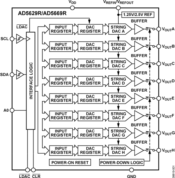
EVAL-AD5669RSDZ
Analog Devices Inc.The AD5669R device is a low power, octal, 16-bit, buffered voltage-output DACs. It operates from a single 2.7 V to 5.5 V supply and is guaranteed monotonic by design.The AD5629R/AD5669R have an on-chip reference with aninternal gain of 2. The AD5629R-1/AD5669R-1 have a 1.25 V,5 ppm/?C reference, giving a full-scale output range of 2.5 V.The AD5629R-2/AD5629R-3 and the AD5669R-2/AD5669R-3have a 2.5 V 5 ppm/?C reference, giving a full-scale output rangeof 5 V depending on the option selected. Devices with 1.25 Vreference selected operate from a single 2.7 V to 5.5 V supply.Devices with 2.5 V reference selected operate from 4.5 V to 5.5 V.The on-chip reference is off at power-up, allowing the use of anexternal reference. The internal reference is enabled via asoftware write.The part incorporates a power-on reset circuit that ensures that the DAC output powers up to 0 V and remains powered up at this level until a valid write takes place. The part contains a power-down feature that reduces the current consumption of the device to 400 nA at 5 V and provides software-selectable output loads while in power-down mode for any or all DAC channels.Product Highlights Octal, 16-bit DACs. On-chip 1.25 V/2.5 V, 5 ppm/?C reference. Available in 16-lead LFCSP and TSSOP, and 16-ball WLCSP. Power-on reset to 0 V or midscale. Power-down capability. When powered down, the DAC typically consumes 200 nA at 3 V and 400 nA at 5 V.Applications Process control Data acquisition systems Portable battery-powered instruments Digital gain and offset adjustment Programmable voltage and current sources

EVAL-AD5676RSDZ
Analog Devices Inc.The AD5672R/AD5676R are low power, octal, 12-/16-bit buffered voltage output digital-to-analog converters (DACs). They include a 2.5 V, 2 ppm/?C internal reference (enabled by default) and a gain select pin giving a full-scale output of 2.5 V (gain = 1) or 5 V (gain = 2). The devices operate from a single 2.7 V to 5.5 V supply and are guaranteed monotonic by design. The AD5672R/AD5676R are available in a 20-lead TSSOP?and in a 20-lead LFCSP and incorporate a power-on reset circuit and a RSTSEL pin that ensures that the DAC outputs power up to zero scale or midscale and remains there until a valid write. The AD5672R/AD5676R contain a power-down mode, reducing the current consumption to 1 ?A typical while in power-down mode. The AD5676R is also available in a 16-ball WLCSP.PRODUCT HIGHLIGHTS High Relative Accuracy (INL). AD5672R (12-bit): ?1 LSB maximum AD5676R (16-bit): ?3 LSB maximum Low Drift 2.5 V On-Chip Reference. High Channel Density.Eight channels in 2.5 mm ? 2.4 mm WLCSP (AD5676R).APPLICATIONS Optical transceivers Base-station power amplifiers Process control (PLC input/output cards) Industrial automation Data acquisition systems

EVAL-AD5676SDZ
Analog Devices Inc.The AD5676 is a low power, octal, 16-bit buffered voltage output digital-to-analog converter (DAC). The device includes a gain select pin, giving a full-scale output of VREF (gain = 1) or 2 ? VREF (gain = 2). The AD5676 DAC operates from a single 2.7 V to 5.5 V supply and is guaranteed monotonic by design. The AD5676 is available in 20-lead TSSOP and LFCSP packages.The internal power-on reset circuit and the RSTSEL pin of the AD5676 ensure that the output DACs power up to zero scale or midscale and then remain there until a valid write takes place. The AD5676 contains a per channel power-down mode that typically reduces the current consumption of the device to 1 ?A.The AD5676 employs a versatile serial peripheral interface (SPI) that operates at clock rates up to 50 MHz, and contains a VLOGIC pin intended for 1.62 V to 5.5 V logic.Product Highlights High Relative Accuracy (INL) 16-bit: ?3 LSB maximum ?40?C to +125?C temperature range 20-lead, TSSOP and LFCSP RoHS-compliant packagesApplications Optical transceivers Base-station power amplifiers Process control (PLC input/output cards) Industrial automation Data acquisition systems

EVAL-AD5693RSDZ
Analog Devices Inc.The AD5693R / AD5692R / AD5691R / AD5693, members of thenanoDAC+? family, are low power, single-channel, 16-/14-/12-bitbuffered voltage output DACs. The devices, except the AD5693,include an enabled by default internal 2.5 V reference, offering2 ppm/?C drift. The output span can be programmed to be 0 V toVREF or 0 V to 2 ? VREF. All devices operate from a single 2.7 V to5.5 V supply and are guaranteed monotonic by design. Thedevices are available in a 2.00 mm ? 2.00 mm, 8-lead LFCSP ora 10-lead MSOP.The internal power-on reset circuit ensures that the DAC registeris written to zero scale at power-up while the internal outputbuffer is configured in normal mode. The AD5693R / AD5692R / ?AD5691R / AD5693 contain a power-down mode that reduces thecurrent consumption of the device to 2 ?A (maximum) at 5 V andprovides software selectable output loads.The AD5693R / AD5692R / AD5691R / AD5693 use an I2Cinterface. Some device options also include an asynchronousRESET pin and a VLOGIC pin, allowing 1.8 V compatibility.Product Highlights High relative accuracy (INL): ?2 LSB maximum (AD5693R/AD5693, 16-bit). Low drift, 2.5 V on-chip reference: 2 ppm/?C typical and 5 ppm/?C maximum temperature coefficient. 2 mm ? 2 mm, 8-lead LFCSP and 10-lead MSOP. Applications Process controls Data acquisition systems Digital gain and offset adjustment Programmable voltage sources Optical modules

EVAL-AD5780SDZ
Analog Devices Inc.The AD5780 is a true 18-bit, unbuffered voltage output digitalto-analogconverter (DAC) that operates from a bipolar supplyof up to 33 V. The AD5780 accepts a positive reference inputrange of 5 V to VDD ? 2.5 V and a negative reference input rangeof VSS + 2.5 V to 0 V. Both reference inputs are buffered on chipand external buffers are not required. The AD5780 offers arelative accuracy specification of ?1 LSB maximum range, andoperation is guaranteed monotonic with a ?1 LSB differentialnonlinearity (DNL) maximum range specification.The part uses a versatile 3-wire serial interface that operates atclock rates of up to 35 MHz and is compatible with standardserial peripheral interface (SPI), QSPI?, MICROWIRE?, andDSP interface standards. The part incorporates a power-onreset circuit that ensures that the DAC output powers up to 0 Vin a known output impedance state and remains in this stateuntil a valid write to the device takes place. The part providesan output clamp feature that places the output in a defined loadstate.Product Highlights True 18-bit accuracy. Wide power supply range of up to ?16.5 V. ?40?C to +125?C operating temperature range. Low 8 nV/?Hz noise. Low ?0.018 ppm/?C gain error temperature coefficient.Applications Medical instrumentation Test and measurement Industrial control Scientific and aerospace instrumentation Data acquisition systems Digital gain and offset adjustment Power supply control

EVAL-AD7091R-8SDZ
Analog Devices Inc.The AD7091R-2?/?AD7091R-4?/ AD7091R-8 family is a multichannel12-bit, ultralow power, successive approximation analog-to-digitalconverter (ADC) that is available in two, four, or eightanalog input channel options. The AD7091R-2 / AD7091R-4 / AD7091R-8 operate from a single 2.7 V to 5.25 V power supplyand are capable of achieving a sampling rate of 1 MSPS.The AD7091R-2 / AD7091R-4 / AD7091R-8 family offers up to eightsingle-ended analog input channels with a channel sequencerthat allows a preprogrammed selection of channels to be convertedsequentially. The AD7091R-2 / AD7091R-4 / AD7091R-8 alsofeature an on-chip conversion clock, an on-chip accurate 2.5 Vreference, and a high speed serial interface.The AD7091R-2 / AD7091R-4 / AD7091R-8 have a serial portinterface (SPI) that allows data to be read after the conversionwhile achieving a 1 MSPS throughput rate. The conversion processand data acquisition are controlled using the CONVST pin.The AD7091R-2 / AD7091R-4 / AD7091R-8 use advanced designtechniques to achieve ultralow power dissipation at highthroughput rates. They also feature flexible power managementoptions. An on-chip configuration register allows the user to set updifferent operating conditions. These include power management,alert functionality, busy indication, channel sequencing, andgeneral-purpose output pins. The MUXOUT and ADCIN pinsallow signal conditioning of the multiplexer output prior toacquisition by the ADC.APPLICATIONS Battery powered systems Personal digital assistants Medical instruments Mobile communications Instrumentation and control systems Data acquisition systems Optical sensors Diagnostic/monitoring functions

AD7134 Evaluation Board
Analog Devices Inc.The EVAL-AD7134FMCZ evaluation kit features the AD7134 24-bit, 4-channel, simultaneous sampling, 1.5 MSPS precision alias free analog-to-digital converter (ADC). Two on-board AD7134 ADCs are included to demonstrate multidevice simultaneous sampling. The EVAL-AD7134FMCZ draws power from the system demonstration platform (SDP) EVAL-SDP-CH1Z (SDP-H1) board, and the on-board dc-to-dc regulators regulate an external supply of 8 V to 14 V down to 5 V, 1.8 V, and 1.2 V to supply the AD7134 and peripheral components. Both on-board ADCs have a separate reference of 4.096 V generated by the on-board ADR444. The ADCs have three clock input options and can be clocked by a crystal input, a microelectromechanical system (MEMS) oscillator, or a complementary metal-oxide semiconductor (CMOS) clock.
The EVAL-AD7134FMCZ connects to the PC USB port via the SDP-H1 board.
The AD7134 evaluation software running on a PC provides full accessibility to the AD7134 device register map, as well as a data analysis interface to display key parameters and graphics from the conversion result in both time and frequency domains.
For full details on the AD7134, see the AD7134 data sheet, which must be consulted in conjunction with this user guide when using the EVAL-AD7134FMCZ.

EVAL-AD7150EBZ
Analog Devices Inc.The AD7150 delivers a complete signal processing solution for capacitive proximity sensors, featuring an ultralow power converter with fast response time. The AD7151?is a single-channel, lower power alternative to the AD7150.The AD7150 uses Analog Devices, Inc., capacitance-to-digital converter (CDC) technology, which combines features important for interfacing to real sensors, such as high input sensitivity and high tolerance of both input parasitic ground capacitance and leakage current.The integrated adaptive threshold algorithm compensates for any variations in the sensor capacitance due to environmental factors like humidity and temperature or due to changes in the dielectric material over time.By default, the AD7150 operates in standalone mode using the fixed power-up settings and indicates detection on two digital outputs. Alternatively, the AD7150 can be interfaced to a microcontroller via the serial interface, the internal registers can be programmed with user-defined settings, and the data and status can be read from the part.The AD7150 operates with a 2.7 V to 3.6 V power supply. It is specified over the temperature range of ?40?C to +85?C.APPLICATIONS Proximity sensing Contactless switching Position detection Level detection

AD7173-8SDZ Evaluation Board
Analog Devices Inc.The EVAL-AD7173-8SDZ is a fully featured evaluation kit for the AD7173-8. This board operates in stand alone mode or in conjunction with the System Development Platform, EVAL-SDP-CB1Z . When operated with the System Development Platform software is provided enabling the user to perform detailed analysis of the ADC's performance. This software includes the technical note describing the operation and set up of the evaluation board in standalone operation or when operated with the System Development Platform . When operated in standalone mode the ADZS-BRKOUT-EX3 break out board is recommended for access to various control pins.
The SDP Controller board is a separate list item in the ordering guide below (EVAL-SDP-CB1Z). If you have not previously purchased an SDP Controller board, please do so to ensure a full evaluation setup.

EVAL-AD7175-2SDZ
Analog Devices Inc.The AD7175-2 is a low noise, fast settling, multiplexed, 2-/4-channel (fully/pseudo differential) ?-? analog-to-digital converter(ADC) for low bandwidth inputs. It has a maximum channelscan rate of 50 kSPS (20 ?s) for fully settled data. The outputdata rates range from 5 SPS to 250 kSPS.The AD7175-2 integrates key analog and digital signal conditioningblocks to allow users to configure an individual setup foreach analog input channel in use. Each feature can be user selectedon a per channel basis. Integrated true rail-to-rail buffers on theanalog inputs and external reference inputs provide easy to drivehigh impedance inputs. The precision 2.5 V low drift (2 ppm/?C)band gap internal reference (with output reference buffer) addsembedded functionality to reduce external component count.The digital filter allows simultaneous 50 Hz/60 Hz rejection at27.27 SPS output data rate. The user can switch betweendifferent filter options according to the demands of eachchannel in the application. The ADC automatically switchesthrough each selected channel. Further digital processingfunctions include offset and gain calibration registers,configurable on a per channel basis.The device operates with a 5 V AVDD1, or ?2.5 V AVDD1/AVSS,and 2 V to 5 V AVDD2 and IOVDD supplies. The specifiedoperating temperature range is ?40?C to +105?C. The AD7175-2 isin a 24-lead TSSOP package.Applications Process control: PLC/DCS modules Temperature and pressure measurement Medical and scientific multichannel instrumentation Chromatography

EVAL-AD7177-2SDZ
Analog Devices Inc.The AD7177-2 is a 32-bit low noise, fast settling, multiplexed,2-/4-channel (fully/pseudo differential) ?-? analog-to-digitalconverter (ADC) for low bandwidth inputs. It has a maximumchannel scan rate of 10 kSPS (100 ?s) for fully settled data. Theoutput data rates range from 5 SPS to 10 kSPS.The AD7177-2 integrates key analog and digital signal conditioningblocks to allow users to configure an individual setup foreach analog input channel in use. Each feature can be user selectedon a per channel basis. Integrated true rail-to-rail buffers on theanalog inputs and external reference inputs provide easy to drivehigh impedance inputs. The precision 2.5 V low drift (2 ppm/?C)band gap internal reference (with output reference buffer) addsembedded functionality to reduce external component count.The digital filter allows simultaneous 50 Hz and 60 Hz rejectionat a 27.27 SPS output data rate. The user can switch betweendifferent filter options according to the demands of eachchannel in the application. The ADC automatically switchesthrough each selected channel. Further digital processingfunctions include offset and gain calibration registers,configurable on a per channel basis.The device operates with a 5 V AVDD1 supply, or with ?2.5 VAVDD1/AVSS, and 2 V to 5 V AVDD2 and IOVDD supplies.The specified operating temperature range is ?40?C to +105?C.The AD7177-2 is available in a 24-lead TSSOP package.Applications Process control: PLC/DCS modules Temperature and pressure measurement Medical and scientific multichannel instrumentation Chromatography

EVAL-AD7190EBZ
Analog Devices Inc.The AD7190 is a low noise, complete analog front end for high precision measurement applications. It contains a low noise, 24-bit sigma-delta (?-?) analog-to-digital converter (ADC). The on-chip low noise gain stage means that signals of small amplitude can be interfaced directly to the ADC.The device can be configured to have two differential inputs or four pseudo differential inputs. The on-chip channel sequencer allows several channels to be enabled, and the AD7190 sequentially converts on each enabled channel. This simplifies communication with the part. The on-chip 4.92 MHz clock can be used as the clock source to the ADC or, alternatively, an external clock or crystal can be used. The output data rate from the part can be varied from 4.7 Hz to 4.8 kHz.The device has two digital filter options. The choice of filter affects the rms noise/noise-free resolution at the programmed output data rate, the settling time, and the 50 Hz/60 Hz rejection. For applications that require all conversions to be settled, the AD7190 includes a zero latency feature.The part operates with 5 V analog power supply and a digital power supply from 2.7 V to 5.25 V. It consumes a current of 6 mA. It is housed in a 24-lead TSSOP package.APPLICATIONS Weigh scales Strain gauge transducers Pressure measurement Temperature measurement Chromatography PLC/DCS analog input modules Data acquisition Medical and scientific instrumentation

EVAL-AD7276SDZ
Analog Devices Inc.The AD7276 / AD7277?/ AD7278?is a 12-bit, high speed, low power, successive approximation analog-to-digital converters (ADCs). The parts operate from a single 2.35 V to 3.6 V power supply and feature throughput rates of up to 3 MSPS. The parts contain a low noise, wide bandwidth track-and-hold amplifier that can handle input frequencies in excess of 55 MHz.The conversion process and data acquisition are controlled using CS and the serial clock, allowing the devices to interface with microprocessors or DSPs. The input signal is sampled on the falling edge of CS, and the conversion is also initiated at this point. There are no pipeline delays associated with the part.The AD7276 / AD7277 / AD7278 uses advanced design techniques to achieve very low power dissipation at high throughput rates. The reference for the part is taken internally from VDD. This allows the widest dynamic input range to the ADC; therefore, the analog input range for the part is 0 to VDD. The conversion rate is determined by the SCLKPRODUCT HIGHLIGHTS 3 MSPS ADCs in a 6-lead TSOT package AD7276 / AD7277 / AD7278 and AD7476A?/ AD7477A?/ AD7478A?pin-compatible High throughput with low power consumption Flexible power/serial clock speed management. This allows maximum power efficiency at low throughput rates Reference derived from the power supply No pipeline delay. The parts feature a standard successive approximation ADC with accurate control of the sampling instant via a CS input and once-off conversion control.

EVAL-AD7292SDZ
Analog Devices Inc.The AD7292 contains all the functionality required for general-purpose monitoring of analog signals and control of external devices, integrated into a single-chip solution. The AD7292 features an 8-channel, 10-bit SAR ADC, four 10-bit DACs, a ?1?C accurate internal temperature sensor, and 12 GPIOs to aid system monitoring and control.The 10-bit, high speed, low power successive approximation register (SAR) ADC is designed to monitor a variety of single-ended input signals. Differential operation is also available by configuring VIN0 and VIN1 to operate as a differential pair.The AD7292 offers a register programmable ADC sequencer, which enables the selection of a programmable sequence of channels for conversion.Four 10-bit digital-to-analog converters (DACs) provide outputs from 0 V to 5 V. An internal, high accuracy, 1.25 V reference provides a separately buffered reference source for both the ADC and the DACs.A high accuracy band gap temperature sensor is monitored and digitized by the 10-bit ADC to give a resolution of 0.03125?C. The AD7292 also features built-in limit and alarm functions.The AD7292 is a highly integrated solution offered in a 36-lead LFCSP package with an operating temperature range of ?40?C to +125?C.APPLICATIONS Base Station Power Amplifier (PA) Monitoring and Control RF Control Loops Optical Communication System Control General-Purpose System Monitoring and Control


