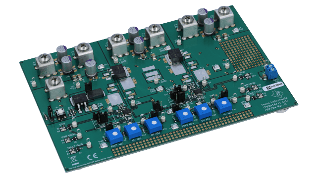
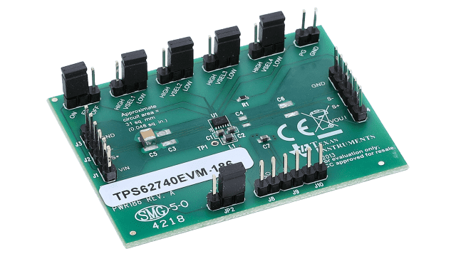
TPS62740EVM-186 Ultra Low Iq Step-Down Converter Low Power Wireless Application Evaluation Module
Texas InstrumentsTPS62740EVM-186 Ultra Low Iq Step-Down Converter Low Power Wireless Application Evaluation Module
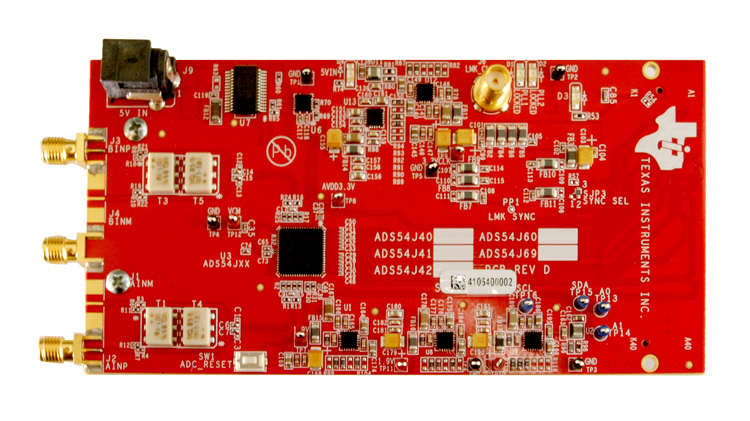
ADS54J20 Dual-Channel; 12-Bit; 1.0-GSPS Analog-to-Digital Converter Evaluation Module
Texas InstrumentsADS54J20 Dual-Channel; 12-Bit; 1.0-GSPS Analog-to-Digital Converter Evaluation Module
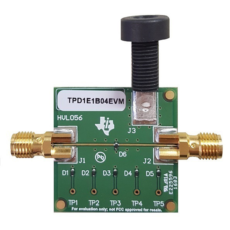
TPD1E1B04 1-Channel ESD Protection Diode With Low RDYN and Low Clamping Voltage Evaluation Module
Texas InstrumentsTPD1E1B04 1-Channel ESD Protection Diode With Low RDYN and Low Clamping Voltage Evaluation Module


EVAL-AD7264EDZ
Analog Devices Inc.The AD7264 is a dual, 14-bit, high speed, low power, successive approximation ADC that operates from a single 5 V power supply and features throughput rates of up to 1 MSPS per on-chip ADC. Two complete ADC functions allow simultaneous sampling and conversion of two channels. Each ADC is preceded by a true differential analog input with a PGA. There are 14 gain settings available: ?1, ?2, ?3, ?4, ?6, ?8, ?12, ?16, ?24, ?32, ?48, ?64, ?96, and ?128.The AD7264 contains four comparators. Comparator A and Comparator B are optimized for low power, whereas Comparator C and Comparator D have fast propagation delays. The AD7264 features a calibration function to remove any device offset error and programmable gain adjust registers to allow input path (for example, sensor) offset and gain compensation. The AD7264 has an on-chip 2.5 V reference that can be disabled if an external reference is preferred. The AD7264 is available in 48-lead LFCSP and LQFP packages.The AD7264 is ideally suited for monitoring small amplitude signals from a variety of sensors. The devices include all the functionality needed for monitoring the position feedback signals from a variety of analog encoders used in motor control systems.Product Highlights Integrated PGA with a variety of flexible gain settings to allow detection and conversion of low level analog signals. Each PGA is followed by a dual simultaneous sampling ADC, featuring throughput rates of 1 MSPS per ADC. The conversion result of both ADCs is simultaneously available on separate data lines or in succession on one data line if only one serial port is available. Four integrated comparators that can be used to count signals from pole sensors in motor control applications. Internal 2.5 V reference.

EVAL-AD7763EDZ
Analog Devices Inc.The AD7763 high performance, 24-bit, ?-? analog-to-digitalconverter (ADC) combines wide input bandwidth and high speed with the benefits of ?-? conversion, as well as performanceof 107 dB SNR at 625 kSPS, making it ideal for high speed dataacquisition. A wide dynamic range, combined with significantly reduced antialiasing requirements, simplifies the design process. An integrated buffer to drive the reference, a differential amplifier for signal buffering and level shifting, an overrange flag, internal gain and offset registers, and a low-pass, digital FIR filter make the AD7763 a compact, highly integrated data acquisition device requiring minimal peripheral componentselection. In addition, the device offers programmable decimation rates and a digital FIR filter, which can be user-programmed to ensure that its characteristics are tailored for the user?s application. The AD7763 is ideal for applications demanding high SNR without necessitating the design of complex, front-end signal processing.The differential input is sampled at up to 40 MSPS by an analogmodulator. The modulator output is processed by a series of low-pass filters, the final filter having default or user-programmable coefficients. The sample rate, filter corner frequencies, and output word rate are set by a combination of the external clock frequency and the configuration registers of the AD7763.The reference voltage supplied to the AD7763 determines theanalog input range. With a 4 V reference, the analog input range is ?3.2 V differential-biased around a common mode of 2 V. This common-mode biasing can be achieved using the on-chip differential amplifiers, further reducing the external signal conditioning requirements.The AD7763 is available in an exposed paddle, 64-lead TQFP_EPand is specified over the industrial temperature range from ?40?C to +85?C.APPLICATIONS Data acquisition systems Vibration analysis Instrumentation
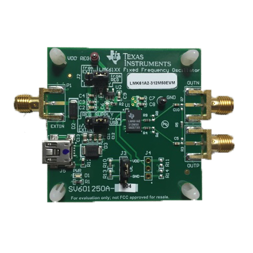
LMK61A2-312M50 Ultra-Low-Jitter Fixed Frequency Oscillator EVM
Texas InstrumentsLMK61A2-312M50 Ultra-Low-Jitter Fixed Frequency Oscillator EVM
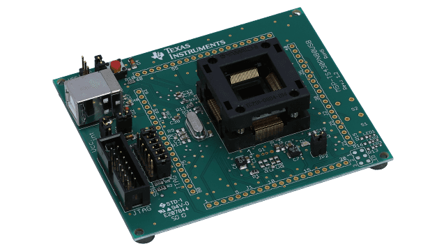
MSP-TS430PN80USB - 80-pin Target Development Board for MSP430F5x MCUs
Texas InstrumentsMSP-TS430PN80USB - 80-pin Target Development Board for MSP430F5x MCUs

124390-HMC741ST89E
Analog Devices Inc.The HMC741 is an InGaP Heterojunction Bipolar Transistor (HBT) Gain Block MMIC SMT amplifier covering 0.05 to 3 GHz. Packaged in an industry standard SOT89, the amplifier can be used as a cascadable 50 Ohm RF or IF gain stage as well as a PA or LO driver with up to +18.5 dBm output power. The HMC741 offers 20 dB of gain with a +42 dBm output IP3 at 200 MHz, and can operate directly from a +5V supply. The HMC741 exhibits excellent gain and output power stability over temperature, while requiring a minimal number of external bias components.Applications Cellular/3G & WiMAX/4G Fixed Wireless & WLAN CATV, Cable Modem & DBS Microwave Radio & Test Equipment IF & RF Applications

124842-HMC794LP3E
Analog Devices Inc.The HMC794LP3E is a SiGe BiCMOS low noise programmable frequency divider in a 3 ? 3mm leadless surface mount package. The circuit can be programmed to divide from N = 1 to N = 4 in the 200 MHz to 2 GHz input frequency range. The high level output power (up to 10 dBm) with a very low SSB phase noise and 50% duty cycle makes this device ideal for low noise clock generation, LO generation and LO drive applications. Configurable bias controls allow power minimization of up to 20%.APPLICATIONS LO Generation with Low Noise Floor Clock Generators Mixer LO Drive Military Applications Test Equipment Sensors

125604-HMC701LP6CE
Analog Devices Inc.The HMC701LP6CE is a SiGe BiCMOS fractional-N frequency synthesizer. The synthesizer includes a 8GHz 16-bit RF N-Divider, a 24-bit delta-sigma modulator, a very low noise digital phase frequency detector (PFD), and a precision controlled charge pump. In addition the synthesizer supports an external step tuned VCO.The fractional synthesizer features an advanced delta-sigma modulator design that allows ultra-fine frequency step sizes. The synthesizer features the ability to alter both the phase-frequency detector (PFD) gain and the cycle slipping characteristics of the PFD. This feature can reduce the time to arrive at the new frequency by 50% vs. conventional PFDs. Ultra low in-close phase noise also allows wider loop bandwidths for faster frequency hopping.The synthesizer contains a built-in linear sweeper function, which allows it to perform frequency chirps with a wide variety of sweep times, polarities and dwells, all with an external or automatic sweep trigger.A General Purpose Output (GPO) bus supports the use of multiple VCOs. In addition the synthesizer has a number of auxiliary clock generation modes that can be accessed via the GPO.Applications Base Stations for Mobile Radio (GSM, PCS, DCS, CDMA, WCDMA) Wireless LANs, WiMax Communications Test Equipment CATV Equipment FMCW Sensors Automotive Radar Phased-Array Systems

125614-HMC851LC3C
Analog Devices Inc.The HMC851LC3C is a XOR/XNOR gate function designed to support data transmission rates of up to 28 Gbps, and clock frequencies as high as 28 GHz. The HMC851LC3C also features an output level control pin, VR, which allows for loss compensation or for signal level optimization.All input signals to the HMC851LC3C are terminated with 50 Ohms to ground on-chip, and may be either AC or DC coupled. The differential outputs of the HMC851LC3C may be either AC or DC coupled. Outputs can be connected directly to a 50 Ohm to ground terminated system, while DC blocking capacitors may be used if the terminating system is 50 Ohms to a nonground DC voltage. The HMC851LC3C operates from a single -3.3V DC supply, and is available in a ceramic RoHS compliant 3x3 mm SMT package.APPLICATIONS RF ATE Applications Broadband Test & Measurement Serial Data Transmission?up to 28 Gbps

125682-HMC789ST89E
Analog Devices Inc.The HMC789ST89E is a high linearity GaAs InGaP HBT gain block MMIC operating from 0.7 to 2.8 GHz and packaged in an industry standard SOT89 package. Utilizing a minimum number of external components and a single +5V supply, the amplifier output IP3 can be optimized to +45 dBm. The high output IP3 and high gain make the HMC789ST89E ideal for use in PA driver & pre-driver applications in Cellular/4G and Fixed Wireless.Applications Cellular/4G Fixed Wireless & WLAN CATV, Cable Modem & DBS Microwave Radio & Test Equipment IF & RF Applications


