
DC450A
Microchip Technology Inc.Diode Array 1 Pair Series Connection 700 V 450A Chassis Mount Module
STEVAL-MKBOXPRO
STMicroelectronicsSensorTile.box PRO IoT Application Multi-Sensor Wireless Box Development Kit
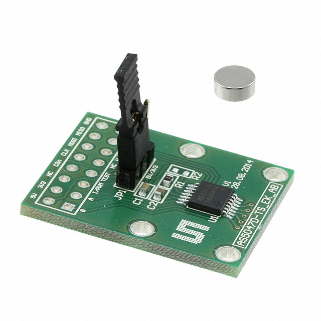
AS5047D-TS_EK_AB
Osram Opto SemiconductorsAS5047D - Magnetic, Rotary Position Sensor Evaluation Board
MPC5746R-252DS
NXP Semiconductors N.V.Daughter Board, MPC5746R, 252 MAPBGA Adapter, MPC5746REVB Evaluation Board
ISL78234EVAL2Z
Renesas Electronics CorporationEvaluation Board, ISL78234AARZ, Synchronous Buck Regulator, Power Management
ISL9104IRUAEVAL1Z
Renesas Electronics CorporationEvaluation Board, ISL9104IRUAZ-T, Step Down Regulator, Power Management
SBC-S32V234
NXP Semiconductors N.V.Single Board Computer, MPX-S32V SoM, Integrated Cooling, ADAS Development
KITVALVECNTLEVM
NXP Semiconductors N.V.Evaluation Kit, MC 34SB0800/34SB0410/9S12XEP/Z33903, Safety System Basis Chip, Power Management
EVAL-L99DZ100G
STMicroelectronicsEvaluation Board, L99DZ100G Door Actuator Driver, Front Door Zone, Automotive
FRDM-GD3100EVM
NXP Semiconductors N.V.Evaluation Board, GD3100 IGBT Gate Driver, Half-Bridge Evaluation, KL25Z Freedom Board
MICROFJ-SMA-40035-GEVB
onsemiEvaluation Board, MicroFJ-40035 SiPM Sensor, 3 x SMA Connectors, Bias Voltage
MICROFJ-SMTPA-30020-GEVB
onsemiEvaluation Board, MicroFJ-30020 SiPM Sensor, 3 x Through Hole Pins, Bias Voltage
MICROFJ-SMTPA-30035-GEVB
onsemiEvaluation Board, MicroFJ-30035 SiPM Sensor, 3 x Through Hole Pins, Bias Voltage
ADM00965
Microchip Technology Inc.Evaluation Board, CL88031 LED Load Board For ADM00963, 13 x Series LEDs, 230V AC
ISL81601EVAL2Z
Renesas Electronics CorporationEvaluation Board, ISL81601FVEZ, Synchronous Buck-Boost Controller, Power Management
ISL81401AEVAL1Z
Renesas Electronics CorporationEvaluation Board, ISL81401AFRZ, Synchronous Buck-Boost Controller, Power Management
EVM54304-MN-00A
Monolithic Power Systems (MPS)Evaluation Kit, MPM54304GMN-0000, Power Management, DC / DC Buck Converter
STEVAL-MKI155V3
STMicroelectronicsMicrophone Coupon Board, 4 x top Port Digital MEMS Mics, 1.64V-3.6V, Omnidirectional Sensitivity


