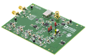
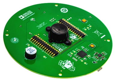
DC871A-C
Analog Devices Inc.The LTC3215 is a low noise, high current charge pump DC/DC converter designed to power high current LEDs. The part includes an accurate programmable current source capable of driving loads up to 700mA from a 2.9V to 4.4V input. Low external parts count (two flying capacitors, one programming resistor and two bypass capacitors) makes the LTC3215 ideally suited for small, battery powered applications.Built-in soft-start circuitry prevents excessive inrush current during start-up. High switching frequency enables the use of small external capacitors. LED current is programmed with an external resistor. The LED is disconnected from VIN during shutdown.An ultralow dropout current source maintains accurate LED current at very low ILED voltages. Automatic mode switching optimizes efficiency by monitoring the voltage across the LED current source and switching modes only when ILED dropout is detected. The LTC3215 is available in a low profile 3mm ? 3mm 10-Lead DFN package.Applications LED Torch/Camera Light Supply for Cell Phones, PDAs and Digital Cameras General Lighting and/or Flash/Strobe Applications
DC875B
Analog Devices Inc.The LTC3454 is a synchronous buck-boost DC/DC converter optimized for driving a single high power LED at currents up to 1A from a single cell Li-Ion battery input. The regulator operates in either synchronous buck, synchronous boost, or buck-boost mode depending on input voltage and LED forward voltage. PLED/PIN efficiency greater than 90% can be achieved over the entire usable range of a Li-Ion battery (2.7V to 4.2V).LED current is programmable to one of four levels, including shutdown, with dual external resistors and dual enable inputs. In shutdown no supply current is drawn. A high constant operating frequency of 1MHz allows the use of small external components.The LTC3454 is offered in a low profile (0.75mm) thermally enhanced 10-lead (3mm ? 3mm) DFN package.Applications Cell Phone Camera Flash Cell Phone Torch Lighting Digital Cameras PDAs Misc Li-Ion LED Drivers
LT3486EFE Demo Board | Dual Boost LED Driver, 3V ≤ VIN ≤ 25V, VLED up to 36V @ 100mA (×2)
Analog Devices Inc.Demonstration circuit 876 is a dual step-up white LED driver with wide dimming range featuring the LT3486. The board is optimized to drive a string of six, eight, or ten white LEDs at 100mA from each of its two outputs with a PVIN input voltage range of 3V to 25V. The maximum LED output voltage must be less than 36V as the overvoltage protection at the output will limit the maximum output voltage to 36V in the case of an open circuit load.
The high input voltage range, high-efficiency low-side internal 1.3A NPN power switches, ground-referenced low-voltage current sense resistors, PWM pins for 1000:1 dimming ratio, control pins for brightness adjust, overvoltage protection, shutdown control pin, externally programmable switching frequency, low shutdown current and internal soft-start capacitor make the LT3486 an extremely powerful and versatile LED driving IC for portable applications and displays.
DC888A-B
Analog Devices Inc.The LTC3706 is a PolyPhase capable secondary-side controller for synchronous forward converters. When used in conjunction with the LTC3705 gate driver and primary-side controller, the part creates a complete isolated power supply that combines the power of PolyPhase operation with the speed of secondary-side control.The LTC3706 has been designed to simplify the design of highly efficient, secondary-side forward converters. Working in concert with the LTC3705, the LTC3706 forms a robust, self-starting converter that eliminates the need for the separate bias regulator that is commonly used in secondary-side control applications. In addition, a proprietary scheme is used to multiplex gate drive signals and DC bias power across the isolation barrier through a single, tiny pulse transformer. The LTC3706 provides remote sensing, accurate power good and overvoltage monitoring circuits to support precision, high current applications. A linear regulator controller with thermal protection is also provided to simplify the generation of secondary-side bias voltage.The LTC3706 is available in a 24-lead SSOP package.Applications Isolated 48V Telecommunication Systems Internet Servers and Routers Distributed Power Step-Down Converters Automotive and Heavy Equipment
DC894C-C
Analog Devices Inc.The LT3825 is an isolated switching regulator controller designed for medium power flyback topologies. A typical application is 10W to 60W with input voltage limited only by external power path components. A third transformer winding provides output voltage feedback.The LT3825 is a current mode controller that regulates output voltage based on sensing secondary voltage via a transformer winding during flyback. This allows for tight output regulation without the use of an opto-isolator, improving dynamic response and reliability. Synchronous rectification increases converter efficiency and improves output cross regulation in multiple output converters.The LT3825 operates in forced continuous conduction mode which improves cross regulation in multiple winding applications. Switching frequency is user programmable and can be externally synchronized. The part also has load compensation, undervoltage lockout and soft-start circuity.Applications Isolated Medium Power (10W to 60W) Supplies Isolated Telecom, Medical Converters Instrumentation Power Supplies Isolated Power over Ethernet Supplies
DC9005B
Analog Devices Inc.SmartMesh IP wireless sensor networks are self managing, low power internet protocol (IP) networks built from wireless nodes called motes. The LTC5800-IPM is the SmartMesh IP integrated circuit in the Eterna? family of IEEE 802.15.4e System-on-Chip (SoC) solutions, featuring a highly integrated, low power radio design as well as an ARM Cortex-M3 32-bit microprocessor running SmartMesh IP embedded networking software.With SmartMesh IP time-synchronized networks, all motes in the network may route, source or terminate data, while providing many years of battery powered operation. SmartMesh IP is a highly flexible network with proven reliability and low power performance in an easy-to-integrate platform.The LTC5800-IPM?s behavior in a SmartMesh IP network is determined by the choice of SmartMesh IP network software loaded: Wireless Mote, EManager, or Access Point Mote in a SmartMesh IP network. The SmartMesh IP software provided with the LTC5800-IPM is fully tested and validated, and is readily configured via a software Application Programming Interface. Once you have purchased SmartMesh IP products, the SmartMesh IP stack binaries may be downloaded via your myAnalog account.The pin signaling behavior of the LTC5800*WR-IPMA hardware is determined by the software loaded and is described in detail in the following product datasheets: LTC5800-IPM = LTC5800*WR-IPMA hardware + SmartMesh IP ?Mote? Software ? LTC5800-IPM Datasheet LTC5800-IPR = LTC5800*WR-IPMA hardware + SmartMesh IP EManager Software ? LTC5800-IPR Datasheet LTC5800-IPA = LTC5800*WR-IPMA hardware + SmartMesh IP Access Point Software ? LTC5800-IPA Datasheet Network Features Feature Benefit >99.999% Network Reliability Avoids communications dropouts common with other wireless networks NIST-certified AES-128 bit Encryption Data protected by end-to-end encryption, message integrity checking and device authentication Scalable Uses time-slotted channel-hopping protocol to avoid in-network collisions to maximize scale while minimizing power and latency-hungry transmission retries due to congestion Bidirectional Communications Ideal for both monitoring and control applications Up to 10 messages/second/node Time-slotted communications avoids contention. This data rate includes built-in margin for packet retries. Device Features Feature Benefit Industry-Leading Low Power Radio Technology ? 4.5mA to Receive a Packet ? 5.4mA to Transmit at 0dBm ? 9.7mA to Transmit at 8dBm Pre-engineered RF RF elements include an on-chip power amplifier and are pre-tuned for optimized performance, including temperature compensation, saving development time. Energy Harvesting Support Very low power design enables motes to be powered by a wide variety of energy harvesters. Click here to see a demonstration circuit of a SmartMesh IP mote powered by indoor light. Integrated Temperature Sensor Precise temperature sensor is integrated directly into the mote. ApplicationsSmartMesh IP is ideally suited for wireless Industrial Internet of Things (IoT) applications. Learn more about SmartMesh applications.?
DC9018B-C
Analog Devices Inc.SmartMesh WirelessHART wireless sensor networks are self managing, low power networks built from wireless nodes called motes. The LTC5800-WHM is the WirelessHART Mote-on-Chip??integrated circuit?in the Eterna? family of IEEE 802.15.4 System-on-Chip (SoC) solutions, featuring a highly integrated, low power radio design by Analog Devices as well as an ARM Cortex-M3 32-bit microprocessor running our embedded SmartMesh WirelessHART networking software.With Analog Devices' time-synchronized WirelessHART networks all motes in the network may route, source or terminate data while providing many years of battery powered operation. The SmartMesh WirelessHART software provided with the LTC5800-WHM is fully tested and validated, and is readily configured via a software Application Programming Interface.SmartMesh WirelessHART motes deliver a highly flexible network with proven reliability and low power performance in an easy-to-integrate platform. Network Features Feature Benefit Time Synchronized, Channel Hopping Communications >99.999% network reliability in even the most challenging RF environments Sub 50 ?A Routers Can build out a network without any line powered devices. Flexibility to be line powered or energy harvested if desired. Secure Mesh with 128-bit AES Encryption NIST Certified Security. Compromise of one node does not compromise network. Standards-based Compliant to international standard IEC 62591 (WirelessHART) Highly Accurate Time Stamping Time stamping on every node is available to applications with millisecond accuracy Device Features Feature Benefit Industry-Leading Low Power Radio Technology 4.5mA to Receive a Packet 5.4mA to Transmit at 0dBm 9.7mA to Transmit at 8dBm Pre-engineered RF RF elements include an on-chip power amplifier and are pre-tuned for optimized performance, including temperature compensation, saving development time. Energy Harvesting Support Very low power design enables motes to be powered by a wide variety of energy harvesters ApplicationsLearn more about SmartMesh applications.
SmartMesh IP RF Certified Eval/Dev Manager (MMCX Antenna Connector), 100 Mote Capacity
Analog Devices Inc.Note: Newer Part Nunber Available - Please see the DC2274A-A
A SmartMesh IP Network Manager anchors the SmartMesh IP product line. It provides core networking functionality, enabling the network to achieve unsurpassed levels of resilience, reliability and scalability, with advanced network management and comprehensive security features.
DC9020B Evaluation/Development Network Manager incorporates the LTP™5902-IPR SmartMesh IP embedded manager (with an MMCX antenna connector) and provides a USB connection for both power and software access to the manager API UART port. Optionally, the DC9006 Eterna interface card (shown on the right hand side in the picture above) can be removed to allow 3V level access to the LTP5902-IPR signals from embedded processors
DC909A
Analog Devices Inc.The LTC3217 is a low noise charge pump DC/DC converter designed to power four high current LEDs. The LTC3217 requires only four small ceramic capacitors and two current set resistors to form a complete LED power supply and current controller.Built-in soft-start circuitry prevents excessive inrush current during start-up and mode changes. High switching frequency enables the use of small external capacitors. Independent high and low current settings are programmed by two external resistors. Shutdown mode and current output levels are selected via two logic inputs.The current through the LEDs is programmed via ISET1 and ISET2. In addition, the brightness can be controlled by pulse width modulation of the EN2 pin.The charge pump optimizes efficiency based on the voltage across the LED current sources. The part powers up in 1x mode and will automatically switch to boost mode whenever any enabled LED current source begins to enter dropout. The first dropout switches the part into 1.5x mode and a subsequent dropout switches the part into 2x mode. The LTC3217 resets to 1x mode whenever the part is shut down.The LTC3217 is available in a low profile 16-lead (3mm ? 3mm ? 0.75mm) QFN package.Applications Multi-LED Camera Light Supply for Cellphones/ DSCs/PDAs
LT5557EUF | 400MHz to 3.8GHz Down Mixer, 1.95GHz RFIN, 240MHz Discrete Matching IF
Analog Devices Inc.DC910A: Demo Board for the LT5557 400MHz to 3.8GHz 3.3V Active Downconverting Mixer.
LT3487EDD Demo Board
Analog Devices Inc.DC912A: Demo Board for the LT3487 Boost and Inverting Switching Regulator for CCD Bias.
DC917A
Analog Devices Inc.The LTC4267 combines an IEEE 802.3af compliant Powered Device (PD) interface with a current mode switching regulator, providing a complete power solution for PD applications. The LTC4267 integrates the 25k? signature resistor, classi?cation current source, thermal overload protection, signature disable and power good signal along with an undervoltage lockout optimized for use with the IEEE-required diode bridge. The precision dual level input current limit allows the LTC4267 to charge large load capacitors and interface with legacy PoE systems.The current mode switching regulator is designed for driving a 6V rated N-channel MOSFET and features programmable slope compensation, soft-start, and constant frequency operation, minimizing noise even with light loads. The LTC4267 includes an onboard error ampli?er and voltage reference allowing use in both isolated and nonisolated con?gurations.The LTC4267 is available in space saving, low pro?le 16-pin SSOP or DFN packages.Applications IP Phone Power Management Wireless Access Points Security Cameras Power over Ethernet
LTC2207 | CMOS Out, 105Msps, 16-Bit ADC, 1MHz < AIN < 70MHz, (Requires DC718)
Analog Devices Inc.DC918C-A: Demo Board for the LTC2207 16-Bit, 105Msps ADC.
DC919A-D
Analog Devices Inc.The LTC2205/LTC2204 are sampling 16-bit A/D converters designed for digitizing high frequency, wide dynamic range signals up to input frequencies of 700MHz. The input range of the ADC can be optimized with the PGA front end.The LTC2205/LTC2204 are perfect for demanding communications applications, with AC performance that includes 79dB SNR and 100dB spurious free dynamic range (SFDR). Ultralow jitter of 90fsRMS allows undersampling of high input frequencies with excellent noise performance. Maximum DC specs include ?4LSB INL, ?1LSB DNL (no missing codes). A separate output power supply allows the CMOS output swing to range from 0.5V to 3.6V.The ENC+ and ENC? inputs may be driven differentially or single-ended with a sine wave, PECL, LVDS, TTL or CMOS inputs. An optional clock duty cycle stabilizer allows high performance at full speed with a wide range of clock duty cycles.Applications Telecommunications Receivers Cellular Base Stations Spectrum Analysis Imaging Systems ATE
LTC2203 | CMOS OUT, DC INPUT, 25Msps 16-Bit ADC, DC < AIN < 70MHz (Requires DC718)
Analog Devices Inc.DC919A-E: Demo Board for the LTC2203 16-Bit, 25Msps ADCs.
LTC2206-14 | CMOS OUT, DC INPUT, 80Msps 14-Bit ADC, DC < AIN < 70MHz (Requires DC718)
Analog Devices Inc.DC919A-H: Demo Board for the LTC2206-14 14-Bit, 80Msps ADC.
DC921A
Analog Devices Inc.The LTC3532 is a high efficiency, fixed frequency, buck-boost DC/DC converter that operates from input voltages above, below or equal to the output voltage. The topology incorporated in the IC provides a continuous transfer function through all operating modes, making the product ideal for single lithium-ion, multicell alkaline or NiMH applications where the output voltage is within the battery voltage range.The device includes two 0.36? N-channel MOSFET switches and two 0.42? P-channel switches. Switching frequencies up to 2MHz are programmed with an external resistor. Quiescent current is only 35?A in Burst Mode operation, maximizing battery life in portable applications. Automatic Burst Mode operation allows the user to program the load current for Burst Mode operation or to control it manually.Other features include a 1?A shutdown, soft-start control, thermal shutdown, and peak current limit. The LTC3532 is available in a low profile (0.75mm) 10-lead (3mm ? 3mm) DFN and 10-lead MSOP packages.Applications Miniature Hard Disk Drive Power Supply MP3 Players Handheld Instruments Digital Cameras Handheld Terminals
DC922A
Analog Devices Inc.The LTC3736-2 is a 2-phase dual synchronous step-down switching regulator controller with tracking that drives external complementary power MOSFETs using few external components. The constant-frequency current mode architecture with MOSFET VDS sensing eliminates the need for sense resistors and improves efficiency. Power loss and noise due to the ESR of the input capacitance are minimized by operating the two controllers out-of-phase.Pulse-skipping operation provides high efficiency at light loads. 100% duty cycle capability provides low dropout operation, extending operating time in battery-powered systems.The switching frequency can be programmed up to 750kHz, allowing the use of small surface mount inductors and capacitors. For noise sensitive applications, the LTC3736-2 switching frequency can be externally synchronized from 250kHz to 850kHz. An internal soft-start, which can be lengthened externally, smoothly ramps the output voltage during start-up.The LTC3736-2 is available in the tiny thermally enhanced (4mm ? 4mm) QFN and 24-lead narrow SSOP packages. Max Current Sense Voltage Burst Mode Soft Start Spread Spectrum LTC3736 204mV Yes No No LTC3736-1 204mV No No Yes LTC3736-2 345mV No Yes No Applications One or Two Lithium-Ion Powered Devices Notebook and Palmtop Computers, PDAs Portable Instruments Distributed DC Power Systems
LTC2607 Demo Board | Dual 16-bit, I2C VOUT DAC (Requires DC2026)
Analog Devices Inc.Demonstration circuit 934A features the LTC2607 dual 16-bit DAC. This device establishes a new board-density benchmark for 16-bit DACs and advances performance standards for output drive, load regulation, and crosstalk in single supply, voltage-output DACs.
LT5571EUF | 900MHz I/Q Modulator w/ Hi-Z & 0.5VDC Bias
Analog Devices Inc.DC944A: Demo Board for the LT5571 620MHz - 1100MHz High Linearity Direct Quadrature Modulator.


