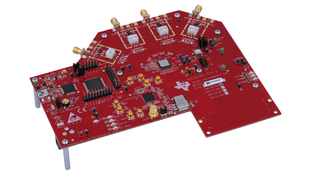
DAC38J84 Quad-Channel; 16-Bit; 2.5-GSPS; 1x-16x Interpolating DAC Evaluation Module
Texas InstrumentsDAC38J84 Quad-Channel; 16-Bit; 2.5-GSPS; 1x-16x Interpolating DAC Evaluation Module
LM3433 4A to 20A LED Driver Evaluation Board
Texas InstrumentsLM3433 4A to 20A LED Driver Evaluation Board
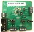
Evaluation Module for BQ24153A Fully Integrated Switch Mode One-Cell Li-Ion Charger
Texas InstrumentsEvaluation Module for BQ24153A Fully Integrated Switch Mode One-Cell Li-Ion Charger
2.7V to 6.5V Input; 3A/2A/2A Buck converter evaluation module
Texas Instruments2.7V to 6.5V Input; 3A/2A/2A Buck converter evaluation module
EVM for 3-A Step-Down Converter in 2x2 mm Package
Texas InstrumentsEVM for 3-A Step-Down Converter in 2x2 mm Package
150-mA, Low-Dropout Regulator Evaluation Module
Texas Instruments150-mA, Low-Dropout Regulator Evaluation Module
LMR16006XEVM 6V to 60V input; 5.0V output at 600mA Step-Down Converter
Texas InstrumentsLMR16006XEVM 6V to 60V input; 5.0V output at 600mA Step-Down Converter
DAC161S997 16-Bit DAC With Internal Reference and 4mA-to-20mA Current Loop Drive Evaluation Module
Texas InstrumentsDAC161S997 16-Bit DAC With Internal Reference and 4mA-to-20mA Current Loop Drive Evaluation Module
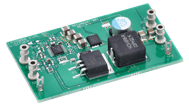
LM25088-1 - Wide Vin Non-Synchronous Buck Controller with Dithering Evaluation Module
Texas InstrumentsLM25088-1 - Wide Vin Non-Synchronous Buck Controller with Dithering Evaluation Module
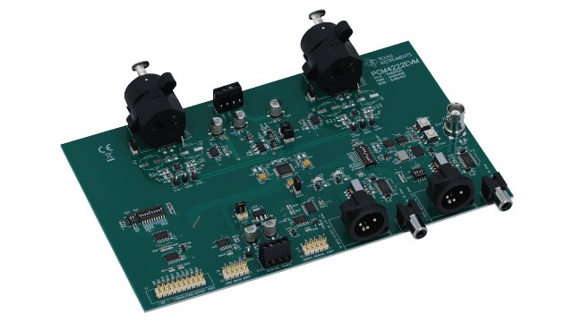
High-Efficiency, Switch-Mode Battery Charge and Power Path Management Evaluation Module
Texas InstrumentsHigh-Efficiency, Switch-Mode Battery Charge and Power Path Management Evaluation Module


