
Search results

2906236
Kemet
0.47 µF ±10% 50V Ceramic Capacitor X7R 1825 (4564 Metric)
| Distributor | SKU | Stock | MOQ | 1 | 10 | 50 | 100 | 1,000 | 10,000 | |
|---|---|---|---|---|---|---|---|---|---|---|
| DigiKey | 399-C1825C474K5RACTUDKR-ND | 665 | $2.18 | $1.28 | $0.95 | $0.95 | $0.77 | $0.77 | Buy |

EVAL-ADATE209BBCZ

Analog Devices Inc.
EVAL-ADATE209BBCZ
Analog Devices Inc.
The ADATE209 is a dual pin driver designed for testing DDR2, DDR3, and DDR4. It can also be used for high speed SoC applications, such as testing PCI Express 1.0 and HDMI?. The device is a three-level driver capable of high fidelity swings from 200 mV to 4 V over a ?1 V to +3.5 V range. It has rise/fall times (20% to 80%) under 120 ps for a 2 V programmed swing and 150 ps for a 3 V programmed swing, and is capable of supporting data rates of 4.4 Gbps and 3.2 Gbps, respectively.The device is capable of high speed transitions into and out of termination mode. It also contains peaking/pre-emphasis circuitry.The ADATE209 is available in an 8 mm ? 8 mm, 49-ball CSP_BGA.APPLICATIONS Automatic test equipment Semiconductor test systems Board test systems Instrumentation and characterization equipment High speed memory testing (DDR2/DDR3/DDR4) HDMI testing
LT3645EMSE Demo Board | VIN = 5V to 36V, VOUT1 = 3.3V @ 300mA, VOUT2= 2.5V @ 200mA

Analog Devices Inc.
LT3645EMSE Demo Board | VIN = 5V to 36V, VOUT1 = 3.3V @ 300mA, VOUT2= 2.5V @ 200mA
Analog Devices Inc.
Demonstration circuit 1428A features the dual output LT3645 step-down regulator plus linear regulator. The circuit is designed to convert a 5V to 36V (55V transients) input source to 3.3V at 500mA using the buck regulator and this output is linear regulated down to provide 2.5V at 200mA. Thus the two outputs provide 300mA (buck) and 200mA (LDO).
33Vin to 60Vin; 12Vout @ 30A; Dual-Phase Synchronous Buck Converter

Texas Instruments
33Vin to 60Vin; 12Vout @ 30A; Dual-Phase Synchronous Buck Converter
Texas Instruments
A dual-phase synchronous buck converter accepting an input voltage of 33Vin to 60Vin and providing an output of 12Vout capable of supplying 30A
85VAC-265VAC Input: 12V/15W Output Green-Mode Flyback

Texas Instruments
85VAC-265VAC Input: 12V/15W Output Green-Mode Flyback
Texas Instruments
The PMP6833 reference design uses the UCC28600 green-mode controller to generate a 12V/15W regulated output. The quasi-resonant switching of the UCC28600 allows this low-cost design to achieve a maximum load efficiency is over 83%: while the no load losses are less than 200mW.
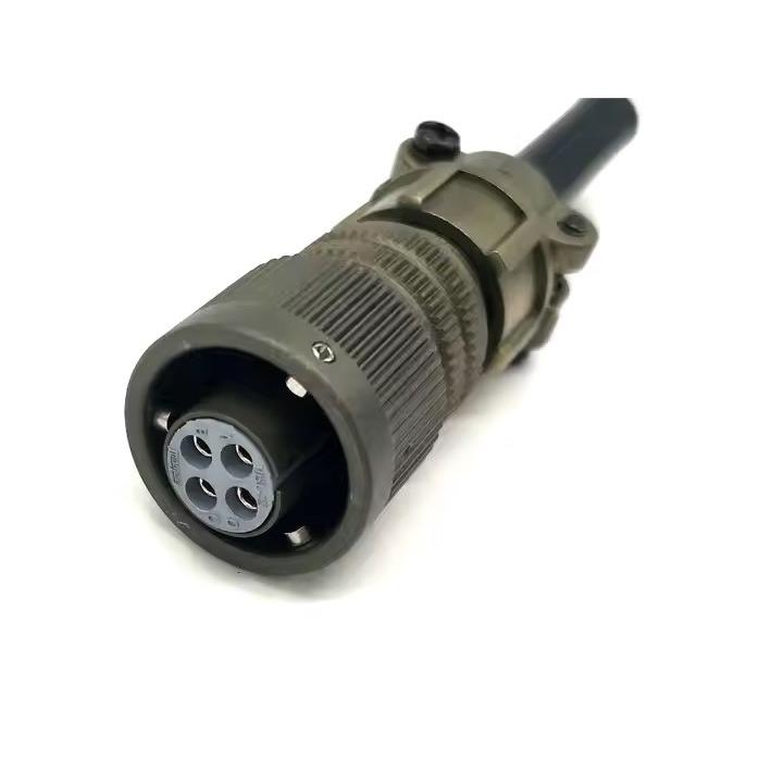
D38999/26JJ37JE
Souriau
37 Position Circular Connector Plug, Female Sockets Crimp
| Distributor | SKU | Stock | MOQ | 1 | 10 | 50 | 100 | 1,000 | 10,000 | |
|---|---|---|---|---|---|---|---|---|---|---|
| DigiKey | 2899-D38999/26JJ37JE-ND | 17 | $292.06 | $268.70 | $247.20 | $227.43 | $227.43 | Buy |
ADP2108-1.5-EVALZ

Analog Devices Inc.
ADP2108-1.5-EVALZ
Analog Devices Inc.
The ADP2108 is a high efficiency, low quiescent current step-down dc-to-dc converter manufactured in two different packages. The total solution requires only three tiny external components. It uses a proprietary, high speed current mode, constant frequency PWM control scheme for excellent stability and transient response. To ensure the longest battery life in portable applications, the ADP2108 has a power save mode that reduces the switching frequency under light load conditions.The ADP2108 runs on input voltages of 2.3 V to 5.5 V, which allows for single lithium or lithium polymer cell, multiple alkaline or NiMH cell, PCMCIA, USB, and other standard power sources. The maximum load current of 600 mA is achievable across the input voltage range.The ADP2108 is available in fixed output voltages of 3.3 V, 3.0 V, 2.5 V, 2.3 V, 1.82 V, 1.8 V, 1.5 V, 1.3 V, 1.2 V, 1.1 V, and 1.0 V. All versions include an internal power switch and synchronous rectifier for minimal external part count and high efficiency. The ADP2108 has an internal soft start and is internally compensated. During logic controlled shutdown, the input is disconnected from the output and the ADP2108 draws less than 1 ?A from the input source.Other key features include undervoltage lockout to prevent deep battery discharge and soft start to prevent input current over-shoot at startup. The ADP2108 is available in 5-ball WLCSP and 5-lead TSOT packages. The ADP2109 provides the same features and operations as the ADP2108 and has the additional function of a discharge switch in the WLCSP package.APPLICATIONS PDAs and palmtop computers Wireless handsets Digital audio, portable media players Digital cameras, GPS navigation units
24VDC 10A eFuse and Protection Circuit for Programmable Logic Controllers (PLC)

Texas Instruments
24VDC 10A eFuse and Protection Circuit for Programmable Logic Controllers (PLC)
Texas Instruments
This sub system design shows an IC based implementation of over voltage: over current: reverse current: reverse polarity and miss wire protection which is more accurate: lower power and faster compared to fuses: PTCs and diodes. Programmable Logic Controller (PLC) I/O modules connected to a field power supply benefit from protection on the 24V field input connectors as power supply faults or miss wiring might damage or cause the module to not operate correctly.
ADP1046ADC1-EVALZ

Analog Devices Inc.
ADP1046ADC1-EVALZ
Analog Devices Inc.
The ADP1046A is a flexible, digital secondary side controller designed for ac-to-dc and isolated dc-to-dc secondary sideapplications. The ADP1046A is pin-compatible with theADP1043A and offers several enhancements and new features,including voltage feedforward and improved loop response to maximize efficiency.The ADP1046A is optimized for minimal component count,maximum flexibility, and minimum design time. Featuresinclude local and remote voltage sense, primary and secondary side current sense, digital pulse-width modulation (PWM)generation, current sharing, and redundant OrFET control. The control loop digital filter and compensation terms are integrated and can be programmed over the I2C interface. Programmableprotection features include overcurrent protection (OCP), over-voltage protection (OVP), undervoltage lockout (UVLO), and overtemperature protection (OTP).The built-in EEPROM provides extensive programming of theintegrated loop filter, PWM signal timing, inrush current, andsoft start timing and sequencing. Reliability is improved through a built-in checksum and programmable protection circuits.A comprehensive GUI is provided for easy design of loop filter characteristics and programming of the safety features.The industry-standard I2C bus provides access to the many monitoring and system test functions.The ADP1046A is available in a 32-lead LFCSP and operatesfrom a single 3.3 V supply.APPLICATIONS AC-to-DC power supplies Isolated dc-to-dc power supplies Redundant power supply systems Server, storage, network, and communications infrastructure
EVAL-AD7843EBZ

Analog Devices Inc.
EVAL-AD7843EBZ
Analog Devices Inc.
The AD7843 is a 12-bit successive-approximation ADC with a synchronous serial interface and low on resistance switches for driving touch screens. The part operates from a single 2.2 V to 5.25 V power supply and features throughput rates greater than 125 kSPS. The external reference applied to the AD7843 can be varied from 1 V to +VCC, while the analog input range is from 0 V to VREF. The device includes a shutdown mode that reduces the current consumption to less than 1 ?A. This part is available in a 16-lead 0.15' Quarter Size Outline (QSOP) package and a 16-lead Thin Shrink Small Outline (TSSOP) package.?Also see the AD7843 sister part, which is the AD7873. This part is similar to the AD7843 but has added functionality such as an on-chip temperature sensor (-40?C to + 85?C), on-chip 2.5 V reference and direct battery and touch-pressure measurement.
LT8644S | 8V, 16A Synchronous Step-Down Silent Switcher 2

Analog Devices Inc.
LT8644S | 8V, 16A Synchronous Step-Down Silent Switcher 2
Analog Devices Inc.
Demonstration circuit 2779A is an 8V, 16A synchronous step-down Silent Switcher® 2 with spread spectrum frequency modulation featuring the LT8644S. The demo board is designed for 1.2V output from a 2.7V to 8V input. The LT8644S is a compact, ultralow emission, high efficiency, and high speed synchronous monolithic stepdown switching regulator. The integrated bypass capacitors optimize all the fast current loops and make it easier to minimize EMI emissions by reducing layout sensitivity. Selectable spread spectrum mode further improves EMI performance, making it perfect solution to the noise sensitive applications. Peak current mode control with minimum on-time of as low as 20ns allows high step-down conversion even at high frequency. The LT8644S switching frequency can be programmed either via an external resistor or an external clock over a 300kHz to 3.5MHz range. The default frequency of demo circuit 2779A is 2MHz. The SYNC/MODE pin on the demo board DC2779A is grounded (JP1 at BURST position) by default for low ripple Burst Mode® operation. It can be configured into different operation modes through JP1 and SYNC terminal (Table 1 in the demo manual). Figure 4 in the demo manual shows the efficiency of the circuit at 3.3V input and 5V input in force continuous mode operation (input from VIN terminal). To get accurate efficiency measurement, measure the input voltage at the VIN_SENSE/GND terminals and measure the output voltage at the VOUT+ SENSE/VOUT– SENSE terminals. Figure 5 shows the LT8644S temperature rise on DC2779A demo board at 3.3V input and 5V input in forced continuous mode. The LT8644S is assembled in a 4mm × 4mm LQFN package with exposed pads for low thermal resistance. The rated maximum continuous load current is 16A, while derating may be necessary for certain input voltage and thermal conditions. The demo board has an EMI filter installed. This EMI filter can be included by applying the input voltage at the VEMI terminal. The EMI performance of the board (with EMI filter) is shown on Figure 6 in the demo manual. The red lines in EMI Performance are CISPR25 Class 5 limits. The figure shows that the LT8644S circuit passes the test with a wide margin. To achieve EMI performance as shown in Figure 6, the input EMI filter is required and the input voltage should be applied to VEMI terminal, and the test setup can be referred to the CISPR25 standards. If the input is applied to VIN terminal, the EMI filter is bypassed. The LT8644S data sheet gives a complete description of the part, the operation and application information. The data sheet must be read in conjunction with the demo manual for demo circuit 2779A. The layout recommendations for low EMI operation and maximum thermal performance are available in the data sheet section Low EMI PCB Layout and Thermal Considerations. Contact ADI applications engineer for support.
EVAL-AD7879-1EBZ

Analog Devices Inc.
EVAL-AD7879-1EBZ
Analog Devices Inc.
The AD7879/AD7889 are 12-bit successive approximationanalog-to-digital converters (SAR ADCs) with a synchronousserial interface and low on-resistance switches for driving 4-wireresistive touch screens. The AD7879/AD7889 work with a verylow power supply?a single 1.6 V to 3.6 V supply?and feature athroughput rate of 105 kSPS. The devices include a shutdownmode that reduces current consumption to less than 6 ?A.To reduce the effects of noise from LCDs and other sources, theAD7879/AD7889 contain a preprocessing block. Thepreprocessing function consists of a median filter and anaveraging filter. The combination of these two filters provides amore robust solution, discarding the spurious noise in the signaland keeping only the data of interest. The size of both filters isprogrammable. Other user-programmable conversion controlsinclude variable acquisition time and first conversion delay; upto 16 averages can be taken per conversion. The AD7879/AD7889can run in slave mode or standalone (master) mode, using anautomatic conversion sequencer and timer.The AD7879/AD7889 have a programmable pin that canoperate as an auxiliary input to the ADCs, as a battery monitor,or as a general-purpose input/output (GPIO). In addition, aprogrammable interrupt output can operate in three modes: as ageneral-purpose interrupt to signal when new data is available(DAV), as an interrupt to indicate when limits are exceeded(INT), or as a pen-down interrupt when the screen is touched(PENIRQ). The AD7879/AD7889 offer temperaturemeasurement and touch pressure measurement.The AD7879 is available in a 12-ball, 1.6 mm ? 2 mm WLCSPand in a 16-lead, 4 mm ? 4 mm LFCSP. The AD7889 is availablein a backside coated version of the WLCSP. Both devices supportan SPI interface (AD7879/AD7889) or an I2C interface (AD7879-1/AD7889-1).Applications Personal digital assistants Smart handheld devices Touch screen monitors Point-of-sale terminals Medical devices Cell phones
Bootloading the TMS320C548 Using the BSP in Standard Mode

Texas Instruments
Bootloading the TMS320C548 Using the BSP in Standard Mode
Texas Instruments
This document describes how to create a boot package and bootload one Texas Instruments (TI)(tm) TMS320C548 digital signal processor (DSP) with another TMS320C54x DSP.