
Search results
EVAL-AD7843EBZ

Analog Devices Inc.
EVAL-AD7843EBZ
Analog Devices Inc.
The AD7843 is a 12-bit successive-approximation ADC with a synchronous serial interface and low on resistance switches for driving touch screens. The part operates from a single 2.2 V to 5.25 V power supply and features throughput rates greater than 125 kSPS. The external reference applied to the AD7843 can be varied from 1 V to +VCC, while the analog input range is from 0 V to VREF. The device includes a shutdown mode that reduces the current consumption to less than 1 ?A. This part is available in a 16-lead 0.15' Quarter Size Outline (QSOP) package and a 16-lead Thin Shrink Small Outline (TSSOP) package.?Also see the AD7843 sister part, which is the AD7873. This part is similar to the AD7843 but has added functionality such as an on-chip temperature sensor (-40?C to + 85?C), on-chip 2.5 V reference and direct battery and touch-pressure measurement.
CD74AC04E

L3Harris Technologies, Inc.
From $0.29 • 1 k+ units available from DigiKey
CD74AC04E
L3Harris Technologies, Inc.
Inverter IC 6 Channel - 14-PDIP
| Distributor | SKU | Stock | MOQ | 1 | 10 | 50 | 100 | 1,000 | 10,000 | |
|---|---|---|---|---|---|---|---|---|---|---|
| DigiKey | 2156-CD74AC04E-HC-ND | 9,698 | 1,018 | $0.29 | Buy |
EV-ADF4360-4EB1Z

Analog Devices Inc.
EV-ADF4360-4EB1Z
Analog Devices Inc.
The ADF4360-4 is a fully integrated integer-N synthesizerand voltage-controlled oscillator (VCO). The ADF4360-4 isdesigned for a center frequency of 1600 MHz. In addition, adivide-by-2 option is available, whereby the user gets an RFoutput of between 725 MHz and 875 MHz.Control of all the on-chip registers is through a simple 3-wireinterface. The device operates with a power supply rangingfrom 3.0 V to 3.6 V and can be powered down when not in use.Applications Wireless handsets (DECT, GSM, PCS, DCS, WCDMA) Test equipment Wireless LANs CATV equipment
20W AC/DC PSR isolated LED Driver for T8

Texas Instruments
20W AC/DC PSR isolated LED Driver for T8
Texas Instruments
This reference design demonstrates low cost: high PF LED Driver solution for T8: which includes single stage Flyback with Primary Side Regulation topology using TPS92310. The input range is 85~265Vac and output is 38~42V 420mA or 26~42V 420mA
24VDC 10A eFuse and Protection Circuit for Programmable Logic Controllers (PLC)

Texas Instruments
24VDC 10A eFuse and Protection Circuit for Programmable Logic Controllers (PLC)
Texas Instruments
This sub system design shows an IC based implementation of over voltage: over current: reverse current: reverse polarity and miss wire protection which is more accurate: lower power and faster compared to fuses: PTCs and diodes. Programmable Logic Controller (PLC) I/O modules connected to a field power supply benefit from protection on the 24V field input connectors as power supply faults or miss wiring might damage or cause the module to not operate correctly.
ADAR1000EVAL1Z

Analog Devices Inc.
ADAR1000EVAL1Z
Analog Devices Inc.
The ADAR1000 is a 4-channel, X and Ku frequency band, beamforming core chip for phased arrays. This device operates in half-duplex between receive and transmit modes. In receive mode, input signals pass through four receive channels and are combined and output at the common RF_IO pin. In transmit mode, the RF_IO input signal is split and passes through the four transmit channels. In both modes, the ADAR1000 provides a ?31 dB gain adjustment range and a full 360? phase adjustment range in each radio frequency (RF) channel, with 6-bit resolution (less than ?0.5 dB and 2.8?, respectively).A simple 4-wire serial port interface (SPI) controls all of the on-chip registers. In addition, two address pins allow SPI control of up to four devices on the same serial lines. Dedicated transmit and receive load pins also provide synchronization of all ADAR1000 chips in the same array, and a single pin controls fast switching between the transmit and receive modes. The ADAR1000 is fabricated in a silicon-germanium, bipolar CMOS (BiCMOS) process. The device is available in a compact, 88-terminal, 7 mm ? 7 mm, LGA package and is specified from ?40?C to +85?C.APPLICATIONS Phased array radar Satellite communications systems
Power for Altera Cyclone V (Cyclone 5) FPGA (.75V@.75A) Reference Design

Texas Instruments
Power for Altera Cyclone V (Cyclone 5) FPGA (.75V@.75A) Reference Design
Texas Instruments
PMP8571 is an easy to use power solution designed using integrated inductor power modules for Altera’s Cyclone 5 FPGA. This design used TPS84621 and TPS84320 along with TPS51200 to generate 5 rails to power the FPGA.
18Vdc-60Vdc Input: 3.3V @ 30A Output: 93% Efficient Active Clamp Forward

Texas Instruments
18Vdc-60Vdc Input: 3.3V @ 30A Output: 93% Efficient Active Clamp Forward
Texas Instruments
The PMP8252 reference design provides 3.3V at 30A from a wide range 18V-60V telecom input with a peak efficiency that is greater than 93%. This design uses the UCC2897A active clamp controller along with Texas Instruments' NexFET power MOSFETs for synchronous rectification.

VLF10045T-680M1R6
TDK Corporation
Ind Power Shielded Wirewound 68uH 20% 100KHz 1.7A T/R
| Distributor | SKU | Stock | MOQ | 1 | 10 | 50 | 100 | 1,000 | 10,000 | |
|---|---|---|---|---|---|---|---|---|---|---|
| DigiKey | 445-3583-2-ND | 0 | Buy | |||||||
| Mouser Electronics | 810-VLF10045T680M1R6 | 0 | 1 | |||||||
| AVNET Express | VLF10045T-680M1R6 | 0 | 500 | Buy | ||||||
| Newark | VLF10045T-680M1R6 | 0 | 1 | $0.00 | $0.00 | $0.00 | $0.00 | $0.00 | $0.00 | Buy |
| Win Source | VLF10045T-680M1R6 | 1,700 | 1 | Buy | ||||||
| Quarktwin Electronic Components | VLF10045T-680M1R6 | 21,534 | 10 | Buy |

High-Speed ADC THS1041 and FPGA Interface Considerations

Texas Instruments
High-Speed ADC THS1041 and FPGA Interface Considerations
Texas Instruments
The Texas Instruments THS1041 is a 10-bit, 40-MSPS, high-speed analog-to-digital converter (ADC). For many years because of its low power dissipation and extended life, it has been used in various applications such as programmable gain amplifier and built-in clamp. With recent FPGA development, some application systems have been upgraded with a direct interface of the THS1041 to an FPGA, for example, by connecting I/O pins of the THS1041 to the I/O pins of Xilinx™ Spartan-3 or Altera™ program logic device (PLD). For such an interface, a power-on initial state should be considered in the interface design. Otherwise, the power-on initial state of the FPGA can affect the initial state of THS1041 and in some cases, affect the entire application system. In order to ensure the successful interfacing of the THS1041 to an FPGA, a test was conducted, and this application report presents those results.
Flatlink Data Transmission System Design Overview (Rev. A)
Texas Instruments
Flatlink Data Transmission System Design Overview (Rev. A)
Texas Instruments
FlatLink is a data transmission system that can provide better than a 2:1 reduction in the number of signal lines used for synchronous parallel data bus structures with no loss in data throughput. To do this FlatLink takes single-ended data at clock rates of up to 68 MHz and increases the data signaling rate seven times up to 476 Mbps. The following report provides some design guidelinesfo
MCIMX280DVM4BR
NXP Semiconductors N.V.
From $11.30 • 10 k+ units available from multiple sources
| Distributor | SKU | Stock | MOQ | 1 | 10 | 50 | 100 | 1,000 | 10,000 | |
|---|---|---|---|---|---|---|---|---|---|---|
| DigiKey | 568-15045-6-ND | 2,008 | $18.34 | $14.60 | $10.06 | $12.63 | $11.61 | $7.29 | Buy | |
| Mouser Electronics | 841-MCIMX280DVM4BR | 0 | 1 | $20.09 | $16.97 | $16.97 | $15.09 | $13.74 | $13.74 | |
| AVNET Express | MCIMX280DVM4BR | 11,000 | 1,000 | $12.16 | $11.85 | Buy | ||||
| Newark | MCIMX280DVM4BR | 0 | 1,000 | $14.02 | $14.02 | Buy | ||||
| AVNET Europe | MCIMX280DVM4BR | 3,000 | 1,000 | $26.26 | $16.90 | Buy | ||||
| Arrow North American Components | MCIMX280DVM4BR | 0 | 1,000 | $11.96 | $11.26 | |||||
| Verical Marketplace | MCIMX280DVM4BR | 1,000 | 27 | $14.12 | $13.42 | $12.01 | $11.30 | |||
| Perceptive | MCIMX280DVM4BR | 48,300 | 1 | Buy |
AD9228-65KITZ
Analog Devices Inc.
AD9228-65KITZ
Analog Devices Inc.
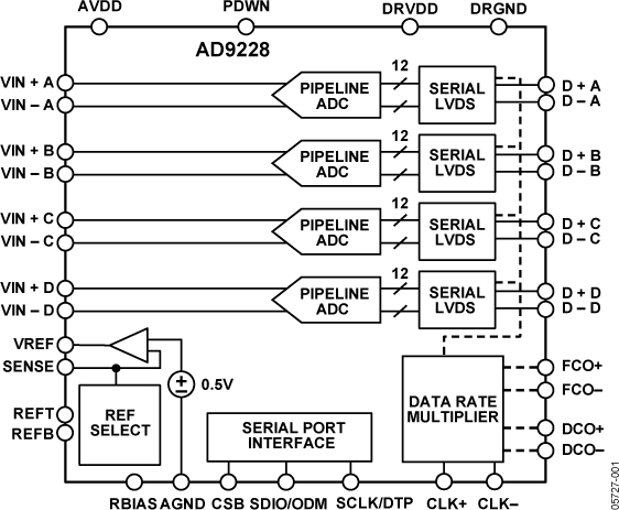
The AD9228 is a quad, 12-bit, 40/65 MSPS analog-to-digital converter (ADC) with an on-chip sample-and-hold circuit designed for low cost, low power, small size, and ease of use. The product operates at a conversion rate of up to 65 MSPS and is optimized for outstanding dynamic performance and low power in applications where a small package size is critical. The ADC requires a single 1.8 V power supply and LVPECL-/ CMOS-/LVDS-compatible sample rate clock for full performance operation. No external reference or driver components are required for many applications. The ADC automatically multiplies the sample rate clock for the appropriate LVDS serial data rate. A data clock output (DCO) for capturing data on the output and a frame clock output (FCO) for signaling a new output byte are provided. Individual channel power-down is supported and typically consumes The ADC contains several features designed to maximize flexibility and minimize system cost, such as programmable clock and data alignment and programmable digital test pattern generation. The available digital test patterns include built-in deterministic and pseudorandom patterns, along with custom user-defined test patterns entered via the serial port interface (SPI). The AD9228 is available in an RoHS compliant, 48-lead LFCSP. It is specified over the industrial temperature range of ?40?C to +85?C.PRODUCT HIGHLIGHTSSmall Footprint. Four ADCs are contained in a small, space-saving package. Low power of 119 mW/channel at 65 MSPS. Ease of Use. A data clock output (DCO) is provided that operates at frequencies of up to 390 MHz and supports double data rate (DDR) operation.User Flexibility. The SPI control offers a wide range of flexible features to meet specific system requirements. Pin-Compatible Family. This includes the AD9287 (8-bit), AD9219 (10-bit), and AD9259 (14-bit).?APPLICATIONSMedical imaging and nondestructive ultrasound Portable ultrasound and digital beam-forming systemsQuadrature radio receivers Diversity radio receivers Tape drives Optical networking Test equipment
0545502071
Molex
From $1.44 • 10 k+ units available from multiple sources
| Distributor | SKU | Stock | MOQ | 1 | 10 | 50 | 100 | 1,000 | 10,000 | |
|---|---|---|---|---|---|---|---|---|---|---|
| DigiKey | WM6791DKR-ND | 0 | $2.72 | $2.09 | $2.20 | $1.72 | $1.36 | $1.33 | Buy | |
| Mouser Electronics | N/A | 0 | ||||||||
| AVNET Express | 0545502071 | 14,336 | 3,000 | $1.34 | Buy | |||||
| AVNET Europe | 0545502071 | 0 | 3,000 | $2.59 | Buy | |||||
| Arrow North American Components | 0545502071 | 0 | 18,000 | |||||||
| Verical Marketplace | 0545502071 | 3,351 | 13 | $0.46 | $0.46 | $0.46 | $0.46 | |||
| Quarktwin Electronic Components | 0545502071 | 36,807 | 10 | $2.43 | $2.19 | $2.19 | $1.97 | $1.59 | $1.44 | Buy |
DC1863A

Analog Devices Inc.
DC1863A
Analog Devices Inc.
The LTC3621/LTC3621-2 is a high efficiency 17V, 1A synchronous monolithic step-down regulator. The switching frequency is fixed to 1MHz or 2.25MHz with a ?40% synchronizing range. The regulator features ultralow quiescent current and high efficiencies over a wide VOUT range.The step-down regulator operates from an input voltage range of 2.7V to 17V and provides an adjustable output range from 0.6V to VIN while delivering up to 1A of output current. A user-selectable mode input is provided to allow the user to trade off ripple noise for light load efficiency; Burst Mode operation provides the highest efficiency at light loads, while pulse-skipping mode provides the lowest voltage ripple. The MODE pin can also be used to allow the user to sync the switching frequency to an external clock. LTC3621 Options Part Name Frequency VOUT LTC3621 1.00MHz Adjustable LTC3621-3.3 1.00MHz 3.3V LTC3621-5 1.00MHz 5V LTC3621-2 2.25MHz Adjustable LTC3621-23.3 2.25MHz 3.3 LTC3621-25 2.25MHz 5V APPLICATIONS Portable-Handheld Scanners Industrial and Embedded Computing Automotive Applications Emergency Radio