
Search results
ADP3367ARZ-REEL7

Analog Devices Inc.
ADP3367ARZ-REEL7
Analog Devices Inc.
The ADP3367 is a low-dropout precision voltage regulator that can supply up to 300 mA output current. It can be used to give a fixed +5 V output with no additional external components or can be adjusted from +1.3 V to +16 V using two external resistors. Fixed or adjustable operation can be selected via the SET input. The low quiescent current (17 µA) in conjunction with the standby or shutdown mode (0.2 µA) makes this device especially suitable for battery powered systems. The dropout voltage when supplying 100 µA is only 15 mV allowing operation with minimal headroom thereby prolonging the useful battery life. At higher output current levels the dropout remains low increasing to just 150 mV when supplying 200 mA. A wide input voltage range from 2.5 V to 16.5 V is allowable. Additional features include a dropout detector and a low supply/battery monitoring comparator. The dropout detector can be used to signal loss of regulation while the low battery detector can be used to monitor the input supply voltage.The ADP3367 is a much improved pin-compatible replacement for the MAX667. Improvements include lower supply current, tighter voltage accuracy and superior line and load regulation. Improved ESD protection (>6000 V) is achieved by advanced voltage clamping structures. The ADP3367 is specified over the industrial temperature range -40°C to +85°C and is available in narrow surface mount (SOIC) packages.ADI’s proprietary Thermal Coastline leadframe used in ADP3367AR packaging, has 30% lower thermal resistance than the standard leadframes. This improvement in heat flow rate results in lower die temperature hence improves reliability.APPLICATIONS Handheld Instruments Cellular Telephones Battery Operated Devices Portable Equipment Solar Powered Instruments High Efficiency Linear Power Supplies
| Distributor | SKU | Stock | MOQ | 1 | 10 | 50 | 100 | 1,000 | 10,000 | |
|---|---|---|---|---|---|---|---|---|---|---|
| DigiKey | 2156-ADP3367ARZ-REEL7-ND | 0 | $4.12 | $4.12 | ||||||
| Mouser Electronics | 584-ADP3367ARZ-R7 | 0 | 1,000 | $3.77 | $3.77 | Buy | ||||
| Newark | ADP3367ARZ-REEL7 | 0 | $2.74 | $2.74 | $2.74 | $2.74 | $2.74 | $2.61 | Buy | |
| Arrow North American Components | ADP3367ARZ-REEL7 | 0 | 1,000 | $4.00 | $4.00 | |||||
| Win Source | ADP3367ARZ-REEL7 | 390 | 5 | Buy | ||||||
| Analog Devices Inc | ADP3367ARZ-REEL7 | 0 | $7.09 | $6.40 | $6.11 | $5.30 | $4.22 | $4.22 | Buy |
Standalone Synchronous Switch-mode Li-Ion Charger with 2A FET Reference Design

Texas Instruments
Standalone Synchronous Switch-mode Li-Ion Charger with 2A FET Reference Design
Texas Instruments
This reference design is a solution for a Li-Ion charge management IC. It has a highly integrated battery charge IC utilizing synchronous switch mode power conversion for efficient and comprehensive charge control of a single cell Li-Ion battery. The solutionprovides a convenient method to evaluate the operation and performance of the IC.
Low Cost 32V@3A Boost Converter Efficiently Powers Inkjet Printer Reference Design

Texas Instruments
Low Cost 32V@3A Boost Converter Efficiently Powers Inkjet Printer Reference Design
Texas Instruments
This boost converter operates from a 24V supply and regulates a 32V@3A output. The converter is designed with low cost in mind: but also delivers 96% efficiency. Aluminum output caps effectively handle large load current transients.
Automotive Power Supply
Texas Instruments
Automotive Power Supply
Texas Instruments
PMP7031 is an automotive dual buck supply with a boost on the input: which enables working down to 3V. It has a low quiesecent current during shutdown and supports various functions needed in an automotive application.
LTC3765EMSE/LTC3766EGN Isolated Demo Board | Forward Converter, 18V ≤ VIN ≤ 72V; VOUT = 12V @ 12.5A

Analog Devices Inc.
LTC3765EMSE/LTC3766EGN Isolated Demo Board | Forward Converter, 18V ≤ VIN ≤ 72V; VOUT = 12V @ 12.5A
Analog Devices Inc.
Demonstration circuit 1739A-B is a 150W isolated forward converter with synchronous rectification featuring the LTC3765/LTC3766. This circuit demonstrates a high level of performance, efficiency, and small solution size attainable using these parts in an active-clamp-reset forward converter power supply. It operates at 240kHz and produces a regulated 12V, 12.5A output from an input voltage range of 18V to 72V, making it well suited for telecom, industrial, and other applications.
Automotive TFT LCD Display Solution

Texas Instruments
Automotive TFT LCD Display Solution
Texas Instruments
This reference design implements a video over LVDS solution for automotive infotainment applications.It highlights the support of multi-touch with haptic feedback: LCD backlight control: and ambient light sensing: without the introduction of dedicated support lines back to the host processor. This design is implemented using two boards. The main electronics board: SAT0059 is where the deserializer: microProcessor: backlight controller: haptics drivers and power supply are located. The LCD interface board: SAT0096: is a physical and electrical interface to a specific LCD panel. It connects to the SAT0059 through a Samtec board to board connector and provides connection points for the LCD panel: touchscreen: backlight connections and haptic drivers. The SAT0096 is designed for a Microtips UMSH-8596MD-20T display. If a different display is to be used: a new LCD Interface board would likely need to be designed.
Increasing ADC603 Input Range
Texas Instruments
Increasing ADC603 Input Range
Texas Instruments
The ADS603 is a 10MHz 12-bit analog-to-digital converter with a ±1.25V input range. Many applications call for a higher input range such as ±2.5V. A resistor divider can be used as an input attenuator to increase the input range. The OPA620 can be used to buffer the input attenuator for high-source-impedance applications. Suggested component values and measured performance results a
Automotive Safety and ADAS Applications Reference Design

Texas Instruments
Automotive Safety and ADAS Applications Reference Design
Texas Instruments
This reference design utilizes the TPS65310A-Q1 device which is a power management unit ideally suited for camera or radar based vision system to support features like lane departure warning: collision avoidance systems: blindspot detection or night vision. Alongside ADAS end-equipment applications: this PMIC is also suitable for safety applications.
ABBK00201209601Y00
Pulse Electronics
From $0.03 • 10 k+ units available from multiple sources
ABBK00201209601Y00
Pulse Electronics
Ferrite Chip Bead 600Ohm 300mA 0.4Ohm Multilayer 2-Pin 0805 T/R
| Distributor | SKU | Stock | MOQ | 1 | 10 | 50 | 100 | 1,000 | 10,000 | |
|---|---|---|---|---|---|---|---|---|---|---|
| DigiKey | 553-ABBK00201209601Y00TR-ND | 0 | 4,000 | $0.03 | Buy | |||||
| AVNET Express | ABBK00201209601Y00 | 0 | 4,000 | Buy | ||||||
| element14 APAC | ABBK00201209601Y00 | 3,320 | 10 | $0.16 | $0.16 | $0.11 | $0.09 | $0.05 | Buy | |
| Newark | ABBK00201209601Y00 | 3,320 | 10 | $0.16 | $0.10 | $0.07 | $0.06 | $0.06 | Buy | |
| Farnell | ABBK00201209601Y00 | 3,320 | 10 | $0.07 | $0.07 | $0.05 | $0.04 | $0.03 | Buy | |
| Arrow Europe | ABBK00201209601Y00 | 56,000 | 4,000 | $0.03 |
LPC54605J256ET100E

NXP Semiconductors N.V.
From $5.92 • 10 k+ units available from multiple sources
LPC54605J256ET100E
NXP Semiconductors N.V.
LPC54605 ARM Cortex Based 32-Bit Microcontroller 180MHz ARM Cortex M4 Core RISC 256KB Flash Memory 136KB RAM 1.8V/2.5V/3.3V Supply Voltage -40°C to 105°C 100-Pin TFBGA Tray
| Distributor | SKU | Stock | MOQ | 1 | 10 | 50 | 100 | 1,000 | 10,000 | |
|---|---|---|---|---|---|---|---|---|---|---|
| DigiKey | LPC54605J256ET100E-ND | 0 | $5.98 | $5.98 | Buy | |||||
| AVNET Express | LPC54605J256ET100E | 520 | 260 | $6.16 | $5.90 | Buy | ||||
| Newark | LPC54605J256ET100E | 0 | 260 | $6.21 | $6.21 | Buy | ||||
| AVNET Europe | LPC54605J256ET100E | 110 | 260 | $12.94 | $8.98 | Buy | ||||
| AVNET Asia Pacific | LPC54605J256ET100E | 520 | 260 | $4.20 | $4.05 | Buy | ||||
| Arrow North American Components | LPC54605J256ET100E | 0 | 260 | $5.74 | $5.40 | |||||
| Verical Marketplace | LPC54605J256ET100E | 9,880 | 260 | $5.92 | $5.92 |
EVAL-AD1937AZ

Analog Devices Inc.
EVAL-AD1937AZ
Analog Devices Inc.
The AD1937 is a high performance, single-chip codec that provides four analog-to-digital converters (ADCs) with differential input and eight digital-to-analog converters (DACs) with differential output, using the Analog Devices, Inc., patented multibit sigma-delta (?-?) architecture. An I2C? port is included, allowing a microcontroller to adjust volume and many other parameters. The AD1937 operates from 3.3 V digital and analog supplies. The AD1937 is available in a 64-lead (differential output) LQFP.The AD1937 is designed for low EMI. This consideration is apparent in both the system and circuit design architectures. By using the on-board PLL to derive the master clock from the LR (frame) clock or from an external crystal, the AD1937 eliminates the need for a separate high frequency master clock and can also be used with a suppressed bit clock. The DACs and ADCs are designed using the latest Analog Devices continuous time architecture to further minimize EMI. By using 3.3 V supplies, power consumption is minimized and further reduces emissions.ApplicationsAutomotive audio systems Home theater systemsSet-top boxesDigital audio effects processorsData Sheet, Rev. 0, 9/08
AN-336 Understanding Integrated Circuit Package Power Capabilities (Rev. A)
Texas Instruments
AN-336 Understanding Integrated Circuit Package Power Capabilities (Rev. A)
Texas Instruments
The short and long term reliability of National Semiconductor's interface circuits like any integrated circuit is very dependent on its environmental condition. Beyond the mechanical/environmental factors nothing has a greater influence on this reliability than the electrical and thermal stress seen by the integrated circuit. Both of these stress issues are specifically addressed on every inter
LT3380 Demo Board | Multi-Output Power Management Solution with 4 Buck Switching and 3 LDO Linear Regulators with I2C
Analog Devices Inc.
LT3380 Demo Board | Multi-Output Power Management Solution with 4 Buck Switching and 3 LDO Linear Regulators with I2C
Analog Devices Inc.
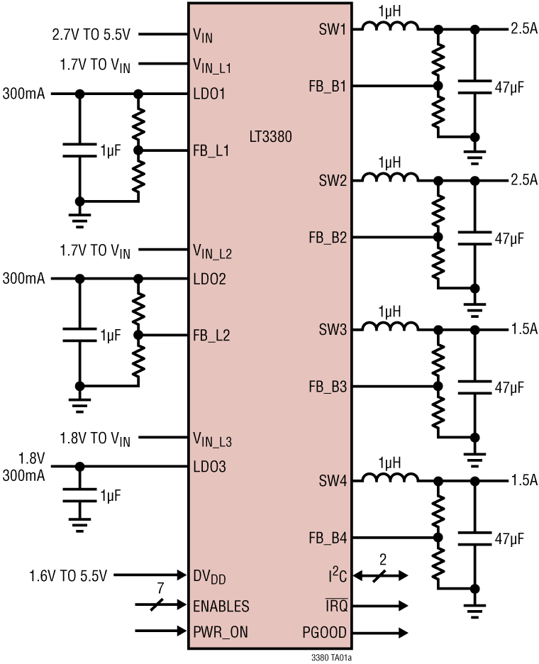
DC2985A is a multi-output power management solution demonstration circuit, featuring the LT3380. It contains two 2.5A, two 1.5A synchronous step-down DC/DC regulators and three 300mA LDO regulators. All regulators can be enabled with external enable pins. After the first regulator is enabled, the remaining enable pins use a precision threshold to allow hardwire-programmed Power-Up Sequence. A micro-USB communication interface is integrated on board to allow software GUI to write or read the registers in LT3380 via its I2C serial port. This GUI can control regulator enables, power-down sequencing, output voltage levels, dynamic voltage scaling, operation modes, status reporting and other special functions. Refer to LT3380 data sheet for more details on the electrical specifications and the setting of its command registers.
Boost Converter LED Driver Using 9V – 24V Input Range

Texas Instruments
Boost Converter LED Driver Using 9V – 24V Input Range
Texas Instruments
This reference design uses the TPS40211 current mode controller in a boost converter to regulate the current in a series string of 12 LEDs (42V) at 0.35A. Efficiency is greater than 94%.
EVAL-ADATE209BBCZ

Analog Devices Inc.
EVAL-ADATE209BBCZ
Analog Devices Inc.
The ADATE209 is a dual pin driver designed for testing DDR2, DDR3, and DDR4. It can also be used for high speed SoC applications, such as testing PCI Express 1.0 and HDMI?. The device is a three-level driver capable of high fidelity swings from 200 mV to 4 V over a ?1 V to +3.5 V range. It has rise/fall times (20% to 80%) under 120 ps for a 2 V programmed swing and 150 ps for a 3 V programmed swing, and is capable of supporting data rates of 4.4 Gbps and 3.2 Gbps, respectively.The device is capable of high speed transitions into and out of termination mode. It also contains peaking/pre-emphasis circuitry.The ADATE209 is available in an 8 mm ? 8 mm, 49-ball CSP_BGA.APPLICATIONS Automatic test equipment Semiconductor test systems Board test systems Instrumentation and characterization equipment High speed memory testing (DDR2/DDR3/DDR4) HDMI testing
Bridgeless Power Factor Correction Converter

Texas Instruments
Bridgeless Power Factor Correction Converter
Texas Instruments
This design is a digitally controlled: bridgeless: 300W: power factor correction (PFC) converter. The distinguishing characteristic of a bridgeless PFC converter is that it eliminates the need for a diode bridge at the input. This reduces power losses that normally occur in a diode bridge and: as a result: improves overall system efficiency. For this design: a C2000™ Piccolo™ TMS320F28035 microcontroller (MCU) is the digital controller for the PFC converter: controlling the two boost power stages that comprise the bridgeless PFC converter. By operating the stages alternatively during the positive and negative half cycles of the AC mains voltage: the Piccolo MCU implements both the AC-to-DC rectification as well as power factor control. This design achieves full load efficiency greater than 93% and power factor of greater than 0.98 at 50% or greater load.
EN55011 Compliant: Industrial Temperature: 10/100Mbps Ethernet PHY Brick Reference Design

Texas Instruments
EN55011 Compliant: Industrial Temperature: 10/100Mbps Ethernet PHY Brick Reference Design
Texas Instruments
This Ethernet PHY Brick reference design enables Texas Instruments customers to quickly design systems and release them to market: using TI industrial Ethernet PHY transceiver devices: fully compliant to EN5501 Class A EMI requirements. A 50 Pin Interface has been provided to interface with 32-Bit Cortex M4 processor based Controller board. The board has been designed in a small form factor (2 inches x 3 inches) which makes it easy to fit into existing products. This reference design demonstrates the advanced performance of the DP83848K Ethernet PHY transceiver devices: supports 10/100 Base-T and is compliant with IEEE 802.3 standard. The entire reference design operates from a single power supply (5V with On-Board regulator or 3.3V). All other voltages required for the Ethernet PHY transceiver are internally generated.