Search results
Using ADS8410/13 in Daisy Chain Mode

Texas Instruments
Using ADS8410/13 in Daisy Chain Mode
Texas Instruments
Many applications require multiple analog-to-digital converters (ADC) in a system. Daisy chaining multiple ADCs enables the use of a single data receiver or a small FPGA. It offers easy and minimal digital routing. This application report describes how multiple ADCs (ADS8410/13) work in a daisy-chain mode. The device offers a high-speed (200 Mbps) LVDS serial interface. This application report als
ADL5500-EVALZ

Analog Devices Inc.
ADL5500-EVALZ
Analog Devices Inc.
The ADL5500 is a mean-responding power detector for use in high frequency receiver and transmitter signal chains from 100 MHz to 6 GHz. It is easy to apply, requiring only a single supply between 2.7 V and 5.5 V and a power supply decoupling capacitor. The input is internally ac-coupled and has a nominal input impedance of 50 ?. The output is a linear-responding dc voltage with a conversion gain of 6.4 V/V rms at 900 MHz. The on-chip, 1 k? series resistance at the output combined with an external shunt capacitor creates a low-pass filter response that reduces the residual ripple in the dc output voltage.The ADL5500 is intended for true power measurement of simple and complex waveforms. The device is particularly useful for measuring high crest factor (high peak-to-rms ratio) signals, such as CDMA2000, W-CDMA, and QPSK/QAM-based OFDM waveforms.The ADL5500 offers excellent temperature stability with near 0 dB measurement error across temperature. The high accuracy range, centered around +3 dBm at 900 MHz, offers ?0.1 dB error from ?40?C to +85?C over an 8.5 dB range. The ADL5500 reduces calibration requirements with low drift across a 30 dB range over temperature and process variations.The ADL5500 operates from ?40?C to +85?C and is available in a 4-ball, 1.0 mm ? 1.0 mm wafer-level chip scale package. It is fabricated on a proprietary high fT silicon bipolar process.
LTC3535EDD Demo Board | Dual Channel 550mA 1MHz Synchronous Step-Up DC/DC Converter

Analog Devices Inc.
LTC3535EDD Demo Board | Dual Channel 550mA 1MHz Synchronous Step-Up DC/DC Converter
Analog Devices Inc.
DC1483A: Demo Board for the LTC3535 Dual Channel 550mA 1MHz Synchronous Step-Up DC/DC Converter.
T556B107M050AT

Kemet
From $26.09 • 10 k+ units available from Quarktwin Electronic Components
| Distributor | SKU | Stock | MOQ | 1 | 10 | 50 | 100 | 1,000 | 10,000 | |
|---|---|---|---|---|---|---|---|---|---|---|
| DigiKey | T556B107M050AT-ND | 0 | 100 | $46.47 | $46.47 | $46.47 | Buy | |||
| Mouser Electronics | 80-T556B107M050AT | 0 | 1 | $52.93 | $47.97 | $44.67 | $43.93 | $43.92 | $43.92 | |
| Newark | T556B107M050AT | 0 | 100 | Buy | ||||||
| Farnell | T556B107M050AT | 0 | 100 | $32.43 | $32.43 | $32.43 | Buy | |||
| Quarktwin Electronic Components | T556B107M050AT | 37,202 | 10 | $44.19 | $39.77 | $39.77 | $35.79 | $28.99 | $26.09 | Buy |
Residential Lighting Gateway for IoT Applications Reference Design

Texas Instruments
Residential Lighting Gateway for IoT Applications Reference Design
Texas Instruments
This design provides a reference ZigBee® gateway for IoT lighting applications. Feature-rich: Linux-based Network & GUI applications powered by Sitara™ AM335x processor can control and monitor ZigBee lighting nodes using the SimpleLink™ ZigBee CC2531 wireless MCU. This design includes example applications for local and remote control of ZigBee nodes: including Android (phones/tablets/set top boxes): Java-script for cloud connectivity agents and C-clients.
Using The 5410 Multi-Channel Buffered Serial Port (McBSP) Sub-Address Scheme
Texas Instruments
Using The 5410 Multi-Channel Buffered Serial Port (McBSP) Sub-Address Scheme
Texas Instruments
Due to memory constraints on data page 0 Multi-Channel Buffered Serial Port (McBSP) registers are accessed using a sub-address scheme. This document discusses how data is accessed through the sub-address registers. A code listing is included.
ADMV1012-EVALZ

Analog Devices Inc.
ADMV1012-EVALZ
Analog Devices Inc.
The ADMV1012 is a compact, gallium arsenide (GaAs) design, monolithic microwave integrated circuit (MMIC) double sideband (DSB) downconverter in a RoHS compliant package optimized for point to point microwave radio designs that operate in the 17.5 GHz to 24 GHz input frequency range. The ADMV1012 provides 15 dB of conversion gain with 25 dB of image rejection, and 2.5 dB noise figure. The ADMV1012 uses a radio frequency (RF) low noise amplifier (LNA) followed by an in phase/quadrature (I/Q), double balanced mixer, where a driver amplifier drives the local oscillator (LO) with a ?2 multiplier. IF1 and IF2 mixer quadrature outputs are provided, and an external 90? hybrid is required to select the required sideband.The I/Q mixer topology reduces the need for filtering of unwanted sideband. The ADMV1012 is a much smaller alternative to hybrid style DSB downconverter assemblies and eliminates the need for wire bonding by allowing the use of surface-mount manufacturing assemblies.The ADMV1012 downconverter comes in a compact, thermally enhanced, 4.9 mm ? 4.9 mm, 32-terminal LCC. The ADMV1012 operates over the ?40?C to +85?C temperature range.Applications Point to point microwave radios Radars and electronic warfare systems Instrumentation, automatic test equipment (ATE)Satellite communications
Interfacing TMS320C5000 DSP to MSP430 Mixed Signal Microcontroller (Rev. A)
Texas Instruments
Interfacing TMS320C5000 DSP to MSP430 Mixed Signal Microcontroller (Rev. A)
Texas Instruments
The TMS320C5000™ family of digital signal processors (DSPs) features Host Port Interface Controllers (HPI) and Direct Memory Access Controllers (DMAC) for efficient data movement without any CPU
GJM0335C1E9R3WB01D

Murata Electronics (UK) Ltd.
From $0.02 • 10 k+ units available from Mouser Electronics
GJM0335C1E9R3WB01D
Murata Electronics (UK) Ltd.
CAP 9.3PF 25V MLCC 0201; Capacitance:9.3pF; Voltage Rating:25V; Ceramic Capacitor Case:0201 [0603 Metric]; Capacitance Tolerance:± 0.05pF; Dielectric Characteristic:C0G / NP0; Product Range:GJM Series; Operating Temperature Min:-55°C; Operating Temperature Max:125°C; Automotive Qualification Standard:-; MSL:MSL 1 - Unlimited; SVHC:No SVHC (27-Jun-2018)
| Distributor | SKU | Stock | MOQ | 1 | 10 | 50 | 100 | 1,000 | 10,000 | |
|---|---|---|---|---|---|---|---|---|---|---|
| DigiKey | 490-GJM0335C1E9R3WB01DTR-ND | 0 | Buy | |||||||
| Mouser Electronics | 81-GJM0335C1E9R3WB1D | 10,575 | 1 | $0.12 | $0.07 | $0.07 | $0.04 | $0.02 | $0.02 | |
| AVNET Express | GJM0335C1E9R3WB01D | 0 | 15,000 | Buy | ||||||
| Farnell | GJM0335C1E9R3WB01D | 0 | 15,000 | Buy | ||||||
| AVNET Asia Pacific | GJM0335C1E9R3WB01D | 0 | 15,000 | Buy |
SEPIC (5V@250mA) for Auxiliary Bias Supply

Texas Instruments
SEPIC (5V@250mA) for Auxiliary Bias Supply
Texas Instruments
The PMP5422 reference design provides an isolated 5V at 250mA from a 120VAC/60Hz input in less than 1 square inch of board space. This design uses the TPS40210 in a non-isolated SEPIC topology. The SEPIC clamping capacitor reduces ringing on the drain of the MOSFET and recaptures leakage energy to improve efficiency.
6 to 16Vin 12V@4A Output Wide Vin SEPIC Converter Reference Design

Texas Instruments
6 to 16Vin 12V@4A Output Wide Vin SEPIC Converter Reference Design
Texas Instruments
This is a Wide-Vin SEPIC converter with an operating input voltage range of 6V to 16V: and implements an output of 12V with the capability of supplying 4A of current to load.
LTC3617EUDD Demo Board | VIN=2.25V to 5.5V, VOUT1 = 0.5VIN (VTT) @ ±6A, VOUT2 = 0.5VIN (VTTR) @ ±10mA

Analog Devices Inc.
LTC3617EUDD Demo Board | VIN=2.25V to 5.5V, VOUT1 = 0.5VIN (VTT) @ ±6A, VOUT2 = 0.5VIN (VTTR) @ ±10mA
Analog Devices Inc.
Demonstration circuit 1707 is a high efficiency monolithic step-down DC/DC switching regulator designed for double-data-rate (DDR) memory termination in computer systems. The VTT output is capable of sourcing and sinking up to 6A with an output voltage equal to one-half the voltage applied to the VDDQIN terminal or one-half the input supply voltage, selected by a jumper. An additional low current output (VTTR) also equal to one-half the voltage on VDDQIN can source and sink up to 10mA. Input voltage range is from 2.25V to 5.5V with overvoltage protection for transients exceeding 6.5V.
AD9959/PCBZ

Analog Devices Inc.
AD9959/PCBZ
Analog Devices Inc.
The AD9959 consists of four direct digital synthesizer (DDS)cores that provide independent frequency, phase, and amplitudecontrol on each channel. This flexibility can be used to correct imbalances between signals due to analog processing, such asfiltering, amplification, or PCB layout-related mismatches.Because all channels share a common system clock, they areinherently synchronized. Synchronization of multiple devices is supported.The AD9959 can perform up to a 16-level modulation of fre-quency, phase, or amplitude (FSK, PSK, ASK). Modulation isperformed by applying data to the profile pins. In addition, theAD9959 also supports linear sweep of frequency, phase, or amplitude for applications such as radar and instrumentation. The AD9959 serial I/O port offers multiple configurations to provide significant flexibility. The serial I/O port offers an SPI-compatible mode of operation that is virtually identical to the SPI operation found in earlier Analog Devices, Inc., DDS products. Flexibility is provided by four data pins (SDIO_0/SDIO_1/SDIO_2/SDIO_3) that allow four programmable modes of serial I/O operation.The AD9959 uses advanced DDS technology that provides low power dissipation with high performance. The device incorporates four integrated, high speed 10-bit DACs with excellent wideband and narrow-band SFDR. Each channel has a dedicated 32-bit frequency tuning word, 14 bits of phase offset, and a 10-bit output scale multiplier. The DAC outputs are supply referenced and must be terminated into AVDD by a resistor or an AVDD center-tapped transformer. Each DAC has its own programmable reference to enable different full-scale currents for each channel. The DDS acts as a high resolution frequency divider with the REFCLK as the input and the DAC providing the output. The REFCLK input source is common to all channels and can be driven directly or used in combination with an integrated REFCLK multiplier (PLL) up to a maximum of 500 MSPS. The PLL multiplication factor is programmable from 4 to 20, in integer steps. The REFCLK input also features an oscillator circuit to support an external crystal as the REFCLK source. The crystal must be between 20 MHz and 30 MHz. The crystal can be used in combination with the REFCLK multiplier.The AD9959 comes in a space-saving 56-lead LFCSP package. The DDS core (AVDD and DVDD pins) is powered by a 1.8 V supply. The digital I/O interface (SPI) operates at 3.3 V and requires DVDD_I/O (Pin 49) be connected to 3.3 V. The AD9959 operates over the industrial temperature range of ?40?C to +85?C.APPLICATIONSAgile local oscillators Phased array radars/sonars Instrumentation Synchronized clocking RF source for AOTF
DC2237A
Analog Devices Inc.
DC2237A
Analog Devices Inc.
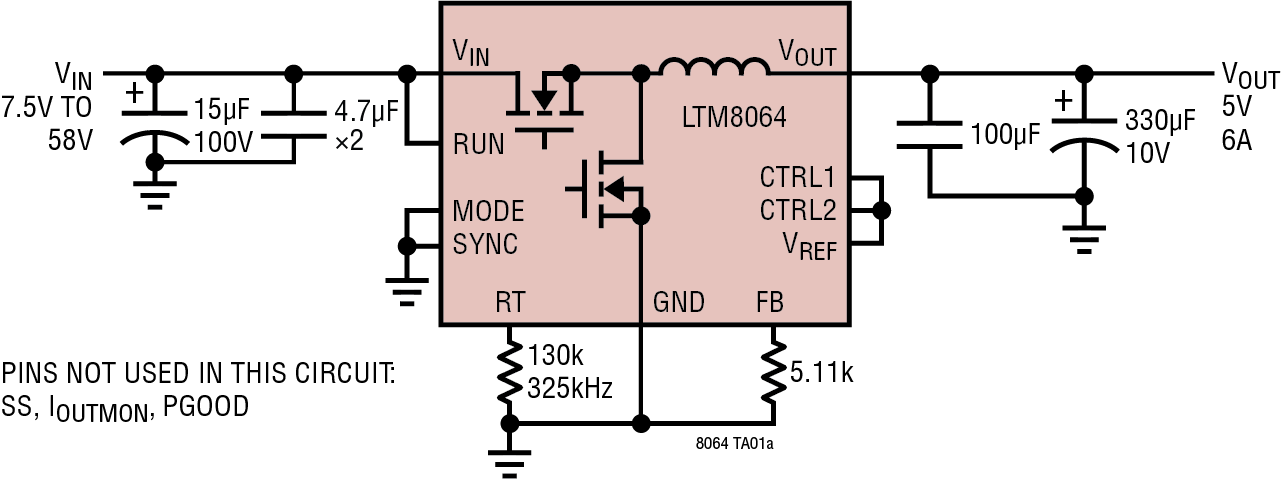
The LTM8064 is a 58VIN, 6A, constant-voltage, constantcurrent (CVCC), step-down ?Module? (power module) regulator. Included in the package are the switching controller, power switches, inductor and support components. Operating over an input voltage range of 6V to 58V, the LTM8064 supports an output voltage range of 1.2V to 36V. CVCC operation allows the LTM8064 to accurately regulate its output current up to 7A when sourcing and 9.1A when sinking over the entire output range. The output current can be set by a control voltage, a single resistor or a thermistor. To set the switching frequency, simply place a resistor from the RT pin to ground. A resistor from FB to ground will set the output voltage. Only the bulk input and output filter capacitors are needed to finish the design.The LTM8064 is packaged in a thermally enhanced, compact (16mm ? 11.9mm ? 4.92mm) over-molded ball grid array (BGA) package suitable for automated assembly by standard surface mount equipment. The LTM8064 is RoHS compliant.Applications Short- Circuit Protection or Accurate Output Current?Limit High Power LED Drive Peltier Driver Motor Drive Battery/Supercap Charging and Cell Balancing