
Search results
ADP5061CB-EVALZ

Analog Devices Inc.
ADP5061CB-EVALZ
Analog Devices Inc.
The ADP5061 charger is fully compliant with USB 3.0 and the USB Battery Charging Specification 1.2 and enables charging via the mini USB VBUS pin from a wall charger, car charger, or USB host port.The ADP5061 operates from a 4 V to 6.7 V input voltage range but is tolerant of voltages up to 20 V. The 20 V voltage tolerance alleviates the concerns about the USB bus spiking during disconnect or connect scenarios.The ADP5061 features an internal FET between the linear charger output and the battery. This permits battery isolation and, hence, system powering under a dead battery or no batteryscenario, which allows for immediate system function on connection to a USB power supply.Based on the type of USB source, which is detected by an external USB detection chip, the ADP5061 can be set to apply the correct current limit for optimal charging and USB compliance.The ADP5061 has three factory programmable digital input/output pins that provide maximum flexibility for different systems. These digital input/output pins permit combinations of features such as, input current limits, charging enable and disable, charging current limits, and a dedicated interrupt output pin. APPLICATIONS Digital still cameras Digital video cameras Single cell Li-Ion portable equipment PDAs, audio, GPS devices Portable medical devices Mobile phones
LT8415EDDB Demo Board | Ultralow Power Boost Converter with Dual Half-Bridge Switches

Analog Devices Inc.
LT8415EDDB Demo Board | Ultralow Power Boost Converter with Dual Half-Bridge Switches
Analog Devices Inc.
DC1449A: Demo Board for the LT8415 Ultralow Power Boost Converter with Dual Half-Bridge Switches.
DC2086A

Analog Devices Inc.
DC2086A
Analog Devices Inc.
The LTM4675 is a dual 9A or single 18A step-down ?Module? (micromodule) DC/DC regulator with 40ms turn-on time. It features remote configurability and telemetry-monitoring of power management parameters over PMBus?an open standard I2C-based digital interface protocol. The LTM4675 is comprised of fast analog control loops, precision mixed-signal circuitry, EEPROM, power MOSFETs, inductors and supporting components.The LTM4675?s 2-wire serial interface allows outputs to be margined, tuned and ramped up and down at programmable slew rates with sequencing delay times. Input and output currents and voltages, output power, temperatures, uptime and peak values are readable. Custom configuration of the EEPROM contents is not required. At start-up, output voltages, switching frequency, and channel phase angle assignments can be set by pin-strapping resistors. The LTpowerPlay? GUI and DC1613 USB-to-PMBus converter and demo kits are available.The LTM4675 is offered in a 16mm ? 11.9mm ? 3.51mm BGA package available with SnPb or RoHS compliant terminal finish.APPLICATIONS System Optimization in Prototype and Production
Using ADS8410/13 in Daisy Chain Mode

Texas Instruments
Using ADS8410/13 in Daisy Chain Mode
Texas Instruments
Many applications require multiple analog-to-digital converters (ADC) in a system. Daisy chaining multiple ADCs enables the use of a single data receiver or a small FPGA. It offers easy and minimal digital routing. This application report describes how multiple ADCs (ADS8410/13) work in a daisy-chain mode. The device offers a high-speed (200 Mbps) LVDS serial interface. This application report als

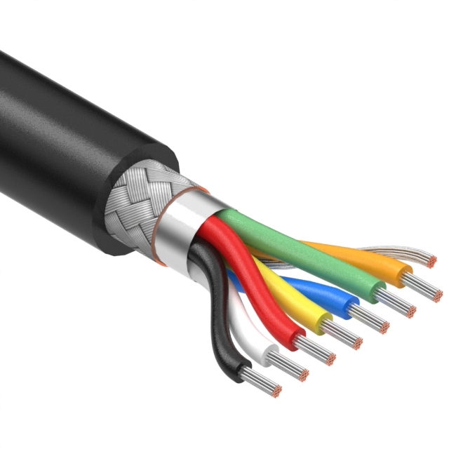
65153
Tensility
7 Conductor Multi-Conductor Cable Black 22 AWG Foil, Braid 502.0' (153.0m)
| Distributor | SKU | Stock | MOQ | 1 | 10 | 50 | 100 | 1,000 | 10,000 | |
|---|---|---|---|---|---|---|---|---|---|---|
| DigiKey | 839-30-01065-153-ND | 2,448 | $4.61 | $4.37 | Buy |


ADAM-5000/TCP
Advantech
8-slot Distributed DA&C System for Ethernet
| Distributor | SKU | Stock | MOQ | 1 | 10 | 50 | 100 | 1,000 | 10,000 | |
|---|---|---|---|---|---|---|---|---|---|---|
| DigiKey | 2084-ADAM-5000/TCP-CE-ND | 2 | 1 | $487.00 | $487.00 | $487.00 | $487.00 | $487.00 | $487.00 | Buy |
| Mouser Electronics | N/A | 0 |
EVAL-ADAQ4001FMCZ

Analog Devices Inc.
EVAL-ADAQ4001FMCZ
Analog Devices Inc.
The ADAQ4001 is a ?Module? precision data acquisition (DAQ), signal chain solution that reduces the development cycle of a precision measurement system by transferring the signal chain design challenge of component selection, optimization, and layout from the designer to the device. Using system-in-package (SIP) technology, the ADAQ4001 reduces end system component count by combining multiple common signal processing and conditioning blocks into a single device. These blocks include a high resolution 16-bit, 2 MSPS successive approximation register (SAR), analog-to-digital converter (ADC), a low noise, fully differential ADC driver amplifier (FDA), and a stable reference buffer. Using Analog Devices, Inc., iPassives? technology, the ADAQ4001 also incorporates crucial passive components with superior matching and drift characteristics to minimize temperature dependent error sources and to offer optimized performance (see Figure 1 in the data sheet). Housing this signal chain solution in a small, 7 mm ? 7 mm, 0.80 mm pitch, 49-ball CSP_BGA enables compact form factor designs without sacrificing performance and simplifies end system bill of materials management. This level of system integration makes the ADAQ4001 much less sensitive to printed circuit board (PCB) layout while still providing flexibility to adapt to a wide range of signal levels. The serial peripheral interface (SPI)-compatible, serial user interface is compatible with 1.8 V, 2.5 V, 3 V, or 5 V logic, using a separate VIO supply. Specified operation of the ADAQ4001 is from ?40?C to +125?C.APPLICATIONSAutomatic test equipmentMachine automationProcess controlsMedical instrumentationDigital control loops
DC2548A

Analog Devices Inc.
DC2548A
Analog Devices Inc.
The LT8672 is an active rectifier controller for reverse input protection. It drives an external N-channel MOSFET to replace a power Schottky diode. Its very low quiescent current and fast transient response meet the tough requirements in automotive applications where AC input signals of up to 100kHz are present. These signals are rectified with minimum power dissipation on the external FET, simplifying thermal management on the PCB.With a drop of only 20mV, the LT8672 solution eases the minimum input voltage requirement during cold crank and start-stop, allowing simpler and more efficient circuits. If the input power source fails or is shorted, a fast turn-off minimizes reverse current transients. An available shutdown mode reduces the quiescent current to 3.5?A.An integrated auxiliary boost regulator provides the required boost voltage to turn the external FET fully on. A power good pin signals when the external FET is ready to take load current.Applications Automotive Battery Protection Industrial Supplies Portable Instrumentation
AD8479R-EBZ

Analog Devices Inc.
AD8479R-EBZ
Analog Devices Inc.
The AD8479 is a difference amplifier with a very high inputcommon-mode voltage range. The AD8479 is a precision devicethat allows the user to accurately measure differential signals inthe presence of high common-mode voltages up to ?600 V.The AD8479 can replace costly isolation amplifiers in applicationsthat do not require galvanic isolation. The device operates overa ?600 V common-mode voltage range and has inputs that areprotected from common-mode or differential mode transientsup to ?600 V.The AD8479 has low offset voltage, low offset voltage drift, low gain drift, low common-mode rejection drift, and excellent common-mode rejection ratio (CMRR) over a wide frequency range.The AD8479 is available in a space-saving 8-lead SOIC package and is operational over the ?40?C to +125?C temperature range.Applications High voltage current sensing Battery cell voltage monitors Power supply current monitors Motor controls Isolation
Interfacing the VCA8613 with High-Speed ADCs
Texas Instruments
Interfacing the VCA8613 with High-Speed ADCs
Texas Instruments
The VCA8613 is an 8-channel variable gain amplifier ideally suited for portable and mid-range ultrasound applications. Each channel consists of a Low Noise Amplifier (LNA) and a Variable Gain Amplifier (VGA). The VGA contains two parts: a voltage-controlled attenuator (VCA) and a programmable gain amplifier (PGA). The PGA output feeds directly into an integrated 2-pole low-pass Butterworth filter.
9-40V Automotive Input: 5V@2.1A Smart USB Charger Reference Design

Texas Instruments
9-40V Automotive Input: 5V@2.1A Smart USB Charger Reference Design
Texas Instruments
This reference design is a complete automotive USB charger solution from the car battery.From a 9V to 40V DC input: this design generates a 5V/2.1A output for smart phones and tablets.
LTM4705 | 20VIN, Dual 5A Step-Down DC/DC μModule Regulator

Analog Devices Inc.
LTM4705 | 20VIN, Dual 5A Step-Down DC/DC μModule Regulator
Analog Devices Inc.
Demonstration circuit 3051A features the LTM4705, a high efficiency dual 5A or single 10A μModule® DC/DC regulator in a compact and low profile 6.25mm × 7.5mm × 3.22mm BGA package. The LTM4705 can take 3.1V to 20V input and generate 0.6V to 5.5V output (stepdown only). The DC3051A demo board is designed to take 6VIN to 20VIN to dual 5A jumper selectable outputs. The board operates by default at a fixed 1MHz and can be synchronized from 1MHz to 3MHz via the MODE/SYNC pin. With its high switching frequency and current mode architecture, a fast transient response to line and load changes is possible without sacrificing stability. The DC3051A can be used in forced continuous mode or pulse-skipping mode for low noise, or in Burst Mode® operation for high efficiency at light loads. Please see the LTM4705 data sheet for more detailed information. It is recommended to read the data sheet for the LTM4705 prior to making any changes to the DC3051A.
Understanding the Functional Enhancements of DSP/BIOS II and Their Utilization
Texas Instruments
Understanding the Functional Enhancements of DSP/BIOS II and Their Utilization
Texas Instruments
Building upon the software foundation architecture of DSP/BIOS DSP/BIOS II extends Texas Instruments? system software capabilities and services to enable the development of more advanced and complex applications; and provide support for traditional concurrent-system design paradigms. This support is a combination of additional software modules and modifications to the kernel to provide preemp