
Search results


EVAL01-HMC987LP5E

Analog Devices Inc.
EVAL01-HMC987LP5E
Analog Devices Inc.
The HMC987LP5E 1-to-9 fanout buffer is designed for low noise clock distribution. It is intended to generate relatively square wave outputs with rise/fall times < 100 ps. The low skew and jitter outputs of the HMC987LP5E, combined with its fast rise/fall times, leads to controllable low-noise switching of downstream circuits such as mixers, ADCs/DACs or SERDES devices. The noise floor is particularly important in these applications, when the clocknetwork bandwidth is wide enough to allow squarewave switching. Driven at 2 GHz, outputs of the HMC987LP5E have a noise floor of ?166 dBc/Hz, corresponding to a jitter density of 0.6 asec/rtHz - or 50 fs over an 8 GHz bandwidth.The input stage can be driven single-ended or differentially, in a variety of signal formats (CML, LVDS, LVPECL or CMOS), AC or DC coupled. The input stage also features adjustable input impedance. It has 8 LVPECL outputs, and 1 CML output with adjustable swing/power-level in 3 dB steps.Individual output stages may be enabled or disabled for power-savings when not required using either hardware control pins, or under control of a serial-port interface.APPLICATIONS SONET, Fibre Channel,?GigE Clock Distribution ADC/DAC Clock Distribution Low Skew and Jitter Clock?or Data Fanout Wireless/Wired Communications Level Translation High Performance Instrumentation Medical Imaging Single-Ended to Differential?Conversion

EVAL-AD4003FMCZ

Analog Devices Inc.
EVAL-AD4003FMCZ
Analog Devices Inc.
The AD4003/AD4007/AD4011 are high accuracy, high speed, low power, 18-bit, Easy Drive, precision successive approximation register (SAR) analog-to-digital converters (ADCs) that operate from a single power supply, VDD. The reference voltage, VREF, is applied externally and can be set independent of the supply voltage. The AD4003/AD4007/AD4011 power scales linearly with throughput. Easy Drive features reduce both signal chain complexity and power consumption while enabling higher channel density. The reduced input current, particularly in high-Z mode, coupled with a long signal acquisition phase, eliminates the need for a dedicated ADC driver. Easy Drive broadens the range of companion circuitry that is capable of driving these ADCs (see Figure 2 in the data sheet).Input span compression eliminates the need to provide a negative supply to the ADC driver amplifier while preserving access to the full ADC code range. The input overvoltage clamp protects the ADC inputs against overvoltage events, minimizing disturbances on the reference pin and eliminating the need for external protection diodes. Fast device throughput up to 2 MSPS allows users to accurately capture high frequency signals and to implement oversampling techniques to alleviate the challenges associated with antialias filter designs. Decreased serial peripheral interface (SPI) clock rate requirements reduce digital input and output power consumption, broadens digital host options, and simplifies the task of sending data across digital isolation. The SPI-compatible serial user interface is compatible with 1.8 V, 2.5 V, 3 V, and 5 V logic by using the separate VIO logic supply.APPLICATIONS Automated test equipment Machine automation Medical equipment Battery-powered equipment Precision data acquisition systems Instrumentation and control systems
0015915069

Molex
From $0.20 • 10 k+ units available from Quarktwin Electronic Components
| Distributor | SKU | Stock | MOQ | 1 | 10 | 50 | 100 | 1,000 | 10,000 | |
|---|---|---|---|---|---|---|---|---|---|---|
| DigiKey | 0015915069-ND | 0 | $0.31 | Buy | ||||||
| Mouser Electronics | N/A | 0 | ||||||||
| AVNET Express | 0015915069 | 0 | 3,000 | Buy | ||||||
| AVNET Europe | 0015915069 | 0 | 1 | $0.83 | Buy | |||||
| Arrow North American Components | 0015915069 | 0 | 6,000 | $0.50 | ||||||
| Heiland | MOL15-91-5069 | 0 | $0.35 | Buy | ||||||
| Quarktwin Electronic Components | 0015915069 | 29,431 | 10 | $0.34 | $0.30 | $0.30 | $0.28 | $0.22 | $0.20 | Buy |
Implementing Continuously Programmable Digital Filters w/ TMS320C30/40 DSP (Rev. A)
Texas Instruments
Implementing Continuously Programmable Digital Filters w/ TMS320C30/40 DSP (Rev. A)
Texas Instruments
Systems engineers must apply real-time digital hardware solutions to signal processing problems to achieve the goals of reliability repeatability and flexibility. DSP offers the only such solution for many applications. Digital filter components are an integral part of many DSP systems. In particular continuously programmable digital filters (CPDFs) offer a broad range of high-tech applicatio

Primary-Side Regulated Flyback for Universal AC Input and 15V/0.25A Output Reference Design

Texas Instruments
Primary-Side Regulated Flyback for Universal AC Input and 15V/0.25A Output Reference Design
Texas Instruments
The PMP9171 reference design uses the UCC28910 primary-side regulated flyback controller with integrated MOSFET to generate a 15V/0.25A output from an univeral AC input with safety isolation rated transformer. 80% efficiency is achieved at full load and less than 130mW power consumption is observed during no load condition.

AN-386 A Non-Complementary Audio Noise Reduction System (Rev. C)
Texas Instruments
AN-386 A Non-Complementary Audio Noise Reduction System (Rev. C)
Texas Instruments
The popularity of companding or complementary noise reduction systems is self-evident. Nearly allmedium to high quality cassette tape decks include either Dolby®B or Dolby C type noise reduction. Ascant few have different systems such as dbx or Hi-Com. The universal appeal of compandors to n.r.system designers is the amount of noise reduction they can offer yet one of the major reasons t
Polarity Correcting Isolated CAN Reference Design

Texas Instruments
Polarity Correcting Isolated CAN Reference Design
Texas Instruments
A ready to use design that efficiently solves the problem of improper installation by adding antiparallel communication channels and appropriate control signal to enable polarity correction for the Controller Area Network (CAN) bus.
EVAL-AD7175-2SDZ

Analog Devices Inc.
EVAL-AD7175-2SDZ
Analog Devices Inc.
The AD7175-2 is a low noise, fast settling, multiplexed, 2-/4-channel (fully/pseudo differential) ?-? analog-to-digital converter(ADC) for low bandwidth inputs. It has a maximum channelscan rate of 50 kSPS (20 ?s) for fully settled data. The outputdata rates range from 5 SPS to 250 kSPS.The AD7175-2 integrates key analog and digital signal conditioningblocks to allow users to configure an individual setup foreach analog input channel in use. Each feature can be user selectedon a per channel basis. Integrated true rail-to-rail buffers on theanalog inputs and external reference inputs provide easy to drivehigh impedance inputs. The precision 2.5 V low drift (2 ppm/?C)band gap internal reference (with output reference buffer) addsembedded functionality to reduce external component count.The digital filter allows simultaneous 50 Hz/60 Hz rejection at27.27 SPS output data rate. The user can switch betweendifferent filter options according to the demands of eachchannel in the application. The ADC automatically switchesthrough each selected channel. Further digital processingfunctions include offset and gain calibration registers,configurable on a per channel basis.The device operates with a 5 V AVDD1, or ?2.5 V AVDD1/AVSS,and 2 V to 5 V AVDD2 and IOVDD supplies. The specifiedoperating temperature range is ?40?C to +105?C. The AD7175-2 isin a 24-lead TSSOP package.Applications Process control: PLC/DCS modules Temperature and pressure measurement Medical and scientific multichannel instrumentation Chromatography
Next-Generation BTL/Futurebus Transceivers Allow Single-Sided SMT Manufacturing (Rev. C)
Texas Instruments
Next-Generation BTL/Futurebus Transceivers Allow Single-Sided SMT Manufacturing (Rev. C)
Texas Instruments
BTL- and Futurebus-compatible transceivers and switching level meet the requirements of today?s high-speed data-communications and provide significant performance advantages over conventional backplane implementations. This document discusses the current and next generation of BTL/Futurebus Transceivers and the design trade-offs required when using these devices.
33Vin to 60Vin; 12Vout @ 30A; Dual-Phase Synchronous Buck Converter

Texas Instruments
33Vin to 60Vin; 12Vout @ 30A; Dual-Phase Synchronous Buck Converter
Texas Instruments
A dual-phase synchronous buck converter accepting an input voltage of 33Vin to 60Vin and providing an output of 12Vout capable of supplying 30A
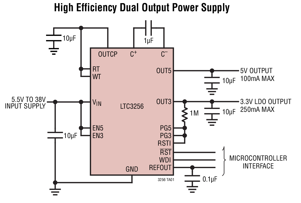
LTC3256 Demo Board | Dual Output Step-Down Charge Pump Plus LDO, 5.5V ≤ VIN ≤ 38V, VOUT1 = 5V @ 100mA, VOUT2 = 3.3V @ 250mA
Analog Devices Inc.
LTC3256 Demo Board | Dual Output Step-Down Charge Pump Plus LDO, 5.5V ≤ VIN ≤ 38V, VOUT1 = 5V @ 100mA, VOUT2 = 3.3V @ 250mA
Analog Devices Inc.
Demonstration Circuit 2375A is a dual output 350mA step down charge pump with a post-regulator LDO and watchdog timer featuring the LTC3256EMSE. The LTC3256 operates with a wide input voltage range from 5.5V to 38V and is engineered for diagnostic coverage in ISO262262 systems. The LTC3256 can provide up to 350mA of output current from a 12V battery with 2W less power dissipation than 2 ideal linear regulators. The DC2375A was populated with automotive grade components for evaluation. Because of the wide input operating range it is possible to exceed the specified operating junction temperature and even reach thermal shutdown with heavy loads. Please refer to the data sheet for additional information on the thermal limitations of the device.
Dynamic Near Field Communication (NFC) Type 4B Tag

Texas Instruments
Dynamic Near Field Communication (NFC) Type 4B Tag
Texas Instruments
This dynamic Near Field Communication (NFC) tag design outlines the required components: layout considerations: and provides firmware examples to implement NFC into applications such as Bluetooth® and Wi-Fi® pairing: equipment configuration and diagnostics: or as a general purpose NFC data interface. The documentation: hardware: and example code provided allows the designer to quickly implement NFC functionality with an MSP430 or other MCU of choice.
A DSP-Based Three-Dimensional Graphics System ( Contains Scanned Text)
Texas Instruments
A DSP-Based Three-Dimensional Graphics System ( Contains Scanned Text)
Texas Instruments
One way to improve the performance of a graphics system is to place an advanced digital signal processor between the host processor and the video controller. This book the author's bachelor's thesis at MIT discusses the suitability of the TMS320C30 Digital Signal Processor to that task.The book begins with a listing of the factors that make the TMS320C30 the digital signal processor of choi