
Search results

LTC4234 Demo Board | 20A Guaranteed SOA Hot Swap Controller

Analog Devices Inc.
LTC4234 Demo Board | 20A Guaranteed SOA Hot Swap Controller
Analog Devices Inc.
Demonstration circuit 2116A features the LTC4233/LTC4234 10A/20A Guaranteed SOA Hot Swap™ Controllers. The LTC4233 and LTC4234 are ideally suited for compact power distribution control in 2.9V to 15V applications for hot board insertion protection, high side power switching, and electronic circuit breaker functions.
PFC Flyback LED Converter 40V - 120V @ 0.35A

Texas Instruments
PFC Flyback LED Converter 40V - 120V @ 0.35A
Texas Instruments
This active power factor correction: transition mode: isolated flyback generates a constant current of 350mA on an LED string from high line (180 to 264Vac). The output accepts a voltage range of 40 to 120V. Open LED protection (overvoltage) and safety discharge of output capacitors are implemented as well.
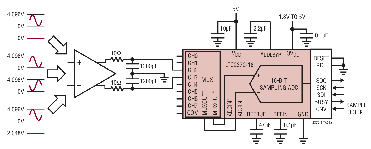
LTC2372-16 Demo Board | 16-Bit, 500ksps, 8-Channel SAR ADC with 96dB SNR (Requires DC590, DC2026 or DC890)
Analog Devices Inc.
LTC2372-16 Demo Board | 16-Bit, 500ksps, 8-Channel SAR ADC with 96dB SNR (Requires DC590, DC2026 or DC890)
Analog Devices Inc.
Demonstration circuit 2071A features the LTC2373 family. The LTC2374/LTC2373/LTC2372 are low noise, high speed, 8-channel, 16/18-bit successive approximation register (SAR) ADCs. The demo manual refers to the LTC2373-18 but applies to all parts in the family, the only differences being the number of bits and the maximum sample rate. Operating from a single 5V supply, the LTC2373-18 has a highly configurable, low crosstalk, 8-channel input multiplexer, supporting fully differential, pseudo-differential unipolar and pseudo-differential bipolar analog input ranges.
Ceramic Capacitors Replace Tantalum Capacitors in LDOs (Rev. A)
Texas Instruments
Ceramic Capacitors Replace Tantalum Capacitors in LDOs (Rev. A)
Texas Instruments
With the proper considerations ceramic output capacitors can be used with low dropout regulators (LDO) and DC/DC switching converters that require tantulum output capacitors.
Respiration Rate Measurement Using Impedance Pneumography
Texas Instruments
Respiration Rate Measurement Using Impedance Pneumography
Texas Instruments
This document discusses the use of impedance pneumography as a technique to measure respiration rate. The generation of high-frequency ac current source is described and the issues related to delay in modulated signal and finite transition times of carriers are addressed. The report also includesdescriptions of potential implementations of a respiration rate measurement system using the ADS1298

Biometric Steering Wheel Reference Design

Texas Instruments
Biometric Steering Wheel Reference Design
Texas Instruments
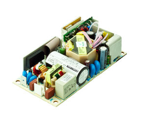
This reference design is for a concept demonstration of how a driver's pulse rate: respiration rate: and ECG based heart rate can be obtained from a vehicle steering wheel. AFE4400 and AFE4300 from TI's biometric family of analog front-ends (AFE): enables acquisition of all three parameters via simple hand contacts on the steering wheel. This reference design also includes a full BLE connectivity design for easy interface to BLE enabled smartphones: tablets: etc
DC2019B

Analog Devices Inc.
DC2019B
Analog Devices Inc.
The LT8614 step-down regulator features Silent Switcher architecture designed to minimize EMI emissions while delivering high efficiency at frequencies up to 3MHz. Assembled in a 3mm ? 4mm QFN, the monolithic construction with integrated power switches and inclusion of all necessary circuitry yields a solution with a minimal PCB footprint. An ultralow 2.5?A quiescent current?with the output in full regulation? enables applications requiring highest efficiency at very small load currents. Transient response remains excellent and output voltage ripple is below 10mVP-P at any load, from zero to full current.The LT8614 allows high VIN to low VOUT conversion at high frequency with a fast minimum top switch on-time of 30ns. Operation is safe in overload even with a saturated inductor.Essential features are included and easy to use: An open-drain PG pin signals when the output is in regulation. The SYNC pin allows clock synchronization and choice of Burst Mode operation or pulse-skipping mode. Soft-start and tracking functionality is accessed via the TR/SS pin. An accurate enable threshold can be set using the EN/UV pin and a resistor at the RT pin programs switch frequency.Applications Automotive and Industrial Supplies General Purpose Step-Down GSM Power Supplies
DC Offset Auto-Calibration of TRF371x
Texas Instruments
DC Offset Auto-Calibration of TRF371x
Texas Instruments
The TRF371x family provides an automatic calibration circuit to minimize the DC offset imbalance in the baseband outputs. This eliminates the dc signal at the ADC output which eats into the valuable dynamic range of the ADC device. This report breaks down the operation of the dc offset calibration and provides the recommended register settings for optimum performance. The convergence time of the c
EVAL-AD4003FMCZ

Analog Devices Inc.
EVAL-AD4003FMCZ
Analog Devices Inc.
The AD4003/AD4007/AD4011 are high accuracy, high speed, low power, 18-bit, Easy Drive, precision successive approximation register (SAR) analog-to-digital converters (ADCs) that operate from a single power supply, VDD. The reference voltage, VREF, is applied externally and can be set independent of the supply voltage. The AD4003/AD4007/AD4011 power scales linearly with throughput. Easy Drive features reduce both signal chain complexity and power consumption while enabling higher channel density. The reduced input current, particularly in high-Z mode, coupled with a long signal acquisition phase, eliminates the need for a dedicated ADC driver. Easy Drive broadens the range of companion circuitry that is capable of driving these ADCs (see Figure 2 in the data sheet).Input span compression eliminates the need to provide a negative supply to the ADC driver amplifier while preserving access to the full ADC code range. The input overvoltage clamp protects the ADC inputs against overvoltage events, minimizing disturbances on the reference pin and eliminating the need for external protection diodes. Fast device throughput up to 2 MSPS allows users to accurately capture high frequency signals and to implement oversampling techniques to alleviate the challenges associated with antialias filter designs. Decreased serial peripheral interface (SPI) clock rate requirements reduce digital input and output power consumption, broadens digital host options, and simplifies the task of sending data across digital isolation. The SPI-compatible serial user interface is compatible with 1.8 V, 2.5 V, 3 V, and 5 V logic by using the separate VIO logic supply.APPLICATIONS Automated test equipment Machine automation Medical equipment Battery-powered equipment Precision data acquisition systems Instrumentation and control systems
3754/30
3M
From $62.40 • 1 k+ units available from multiple sources
| Distributor | SKU | Stock | MOQ | 1 | 10 | 50 | 100 | 1,000 | 10,000 | |
|---|---|---|---|---|---|---|---|---|---|---|
| DigiKey | MB30G-25-ND | 0 | 1 | $39.07 | $29.66 | $24.37 | $22.31 | $22.31 | $22.31 | Buy |
| AVNET Express | 3754/30 | 0 | 10 | $74.98 | $72.13 | $71.03 | $69.36 | $69.36 | Buy | |
| Arrow North American Components | 3754/30 | 2,951 | 1 | $62.40 | $62.40 | $62.40 | $62.40 | $62.40 | ||
| Verical Marketplace | 3754/30 | 2,951 | 1 | $62.40 | $62.40 | $62.40 | $62.40 | $62.40 | $62.40 |
EVAL-AD4114SDZ

Analog Devices Inc.
EVAL-AD4114SDZ
Analog Devices Inc.
The AD4114 is a low power, low noise, 24-bit, sigma-delta (?-?) analog-to-digital converter (ADC) that integrates an analog front end (AFE) for eight fully differential or 16 single-ended, high impedance (?1 M?), bipolar, ?10 V voltage inputs.The AD4114 integrates key analog and digital signal conditioning blocks to configure eight individual setups for each analog input channel in use. The AD4114 features a maximum channel scan rate of 6.21 kSPS (161 ?s) for fully settled data.The embedded 2.5 V, low drift (?5 ppm/?C), band gap internal reference (with output reference buffer) reduces the external component count.The digital filter allows flexible settings, including simultaneous 50 Hz and 60 Hz rejection at a 27.27 SPS output data rate. The user can select different filter settings depending on the requirements of each channel in the application. The automatic channel sequencer enables the ADC to switch through each enabled channel.The precision performance of the AD4114 is achieved by integrating the proprietary iPassives? technology from Analog Devices, Inc. The AD4114 is factory calibrated to achieve a high degree of specified accuracy.The AD4114 operates with a single power supply that allows simplified use in galvanically isolated applications. The specified operating temperature range is ?40?C to +105?C. The AD4114 is housed in a 40-lead, 6 mm ? 6 mm LFCSP.ApplicationsProgrammable logic controller (PLC) and distributed control system (DCS) modules Instrumentation and measurement
EVAL-ADF7021-NDBZ5
Analog Devices Inc.
From $59.85 • 18 units available from multiple sources
EVAL-ADF7021-NDBZ5
Analog Devices Inc.
The ADF7021-N is a high performance, low power, narrow-band transceiver based on the ADF7021. The ADF7021-N has IF filter bandwidths of 9 kHz, 13.5 kHz, and 18.5 kHz, making it ideally suited to worldwide narrowband standards and particularly those that stipulate 12.5 kHz channel separation. It is designed to operate in the narrow-band, license-free ISM bands and in the licensed bands with frequency ranges of 80 MHz to 650 MHz and 842 MHz to 916 MHz. The part has both Gaussian and raised cosine transmit data filtering options to improve spectral efficiency for narrow-band applications. It is suitable for circuit applications targeted at the Japanese ARIB STD-T67, the European ETSI EN 300 220, the Korean short range device regulations, the Chinese short range device regulations, and the North American FCC Part 15, Part 90, and Part 95 regulatory standards. A complete transceiver can be built using a small number of external discrete components, making the ADF7021-N very suitable for price-sensitive and area-sensitive applications. The range of on-chip FSK modulation and data filtering options allows users greater flexibility in their choice of modulation schemes while meeting the tight spectral efficiency requirements. The ADF7021-N also supports protocols that dynamically switch among 2FSK, 3FSK, and 4FSK to maximize communica-tion range and data throughput. The transmit section contains two voltage controlled oscillators (VCOs) and a low noise fractional-N PLL with an output resolution of The frequency-agile PLL allows the ADF7021-N to be used in frequency-hopping, spread spectrum (FHSS) systems. Both VCOs operate at twice the fundamental frequency to reduce spurious emissions and frequency pulling problems. The transmitter output power is programmable in 63 steps from −16 dBm to +13 dBm and has an automatic power ramp control to prevent spectral splatter and help meet regulatory standards. The transceiver RF frequency, channel spacing, and modulation are programmable using a simple 3-wire interface. The device operates with a power supply range of 2.3 V to 3.6 V and can be powered down when not in use. A low IF architecture is used in the receiver (100 kHz), which minimizes power consumption and the external component count yet avoids dc offset and flicker noise at low frequencies. The IF filter has programmable bandwidths of 9 kHz, 13.5 kHz, and 18.5 kHz. The ADF7021-N supports a wide variety of pro-grammable features including Rx linearity, sensitivity, and IF bandwidth, allowing the user to trade off receiver sensitivity and selectivity against current consumption, depending on the application. The receiver also features a patent-pending automatic frequency control (AFC) loop with programmable pull-in range that allows the PLL to track out the frequency error in the incoming signal. The receiver achieves an image rejection performance of 56 dB using a patent-pending IR calibration scheme that does not require the use of an external RF source. An on-chip ADC provides readback of the integrated tempera-ture sensor, external analog input, battery voltage, and RSSI signal, which provides savings on an ADC in some applications. The temperature sensor is accurate to ±10°C over the full oper-ating temperature range of −40°C to +85°C. This accuracy can be improved by performing a 1-point calibration at room temperature and storing the result in memory.
| Distributor | SKU | Stock | MOQ | 1 | 10 | 50 | 100 | 1,000 | 10,000 | |
|---|---|---|---|---|---|---|---|---|---|---|
| DigiKey | EVAL-ADF7021-NDBZ5-ND | 1 | 1 | $88.40 | $88.40 | $88.40 | $88.40 | $88.40 | $88.40 | Buy |
| Mouser Electronics | 584-EVALADF7021NDBZ5 | 4 | 1 | $58.02 | $58.02 | $58.02 | $58.02 | $58.02 | $58.02 | |
| element14 APAC | EVAL-ADF7021-NDBZ5 | 0 | 1 | $119.23 | $119.23 | $119.23 | $119.23 | $119.23 | $119.23 | Buy |
| Farnell | EVAL-ADF7021-NDBZ5 | 0 | 1 | $45.58 | $45.58 | $45.58 | $45.58 | $45.58 | $45.58 | Buy |
| Arrow North American Components | EVAL-ADF7021-NDBZ5 | 0 | 1 | $81.49 | $80.68 | $79.07 | $78.28 | $75.96 | $75.20 | |
| Verical Marketplace | EVAL-ADF7021-NDBZ5 | 13 | 1 | $77.38 | $61.51 | $59.85 | $59.85 | $59.85 | $59.85 | |
| Analog Devices Inc | EVAL-ADF7021-NDBZ5 | 0 | $71.09 | $71.09 | $71.09 | $71.09 | $71.09 | $71.09 | Buy |
Sync Buck for Hard Drive Tester 5V@5A and 3.3V@5A
Texas Instruments
Sync Buck for Hard Drive Tester 5V@5A and 3.3V@5A
Texas Instruments
The PMP3866 reference design is a dual synchronous buck that uses the TPS40140 to generate 5V@5A and 3.3V@5A. The input voltage range is 18V to 30V. This design is used in a hard drive tester application. The two power supplies operate 180 degrees out of phase with each other to reduce the input