
Search results
Primary-Side Regulated Flyback with 85-265VAC Input (24V @ 1.7A) Reference Design

Texas Instruments
Primary-Side Regulated Flyback with 85-265VAC Input (24V @ 1.7A) Reference Design
Texas Instruments
The PMP9041 reference design uses the UCC28710 primary-side regulated flyback controller to generate a 24V/40W output from a univeral AC input. The valley switching of the UCC28710 allows this low-cost design to achieve a maximum load efficiency of 90%; no load losses are less than 50mW.
66470

Desco Industries Inc.
From $1,735.07 • 1 unit available from DigiKey
66470
Desco Industries Inc.
Antistatic Control Products ROLL, STATFREE T2 PLUS RUBBER, DISSIPATIVE, GREEN, 0.060'' x 36'' x 40'
| Distributor | SKU | Stock | MOQ | 1 | 10 | 50 | 100 | 1,000 | 10,000 | |
|---|---|---|---|---|---|---|---|---|---|---|
| DigiKey | 16-66470-ND | 1 | 1 | $1,735.07 | $1,735.07 | $1,735.07 | $1,735.07 | $1,735.07 | $1,735.07 | Buy |
| Mouser Electronics | 809-66470 | 0 | 1 | $1,428.87 | $1,357.41 | $1,357.41 | $1,357.41 | $1,357.41 | $1,357.41 | |
| Newark | 66470 | 0 | 1 | $1,595.47 | $1,595.47 | $1,595.47 | $1,595.47 | $1,595.47 | $1,595.47 | Buy |
Adjusting Amplifier Gain to Achieve Settings Between Preset Gain Steps

Texas Instruments
Adjusting Amplifier Gain to Achieve Settings Between Preset Gain Steps
Texas Instruments
This application report describes two methods to obtain a gain setting for a fixed-gain audio power amplifier. Included is a detailed operation analysis.
DC2966A

Analog Devices Inc.
DC2966A
Analog Devices Inc.
The LTC3376 is a highly flexible multioutput power supply IC. The device includes four synchronous buck converters, configured to share eight 1.5A power stages, powered from independent 3V to 20V inputs. The DC/DCs are assigned to one of fifteen power configurations via pin strappable CFG0 to CFG3 pins. The LTC3376 includes the integration of ceramic capacitors into the package for the BST pins thereby saving PCB space. The common buck switching frequency may be programmed with an external resistor, synchronized to an external oscillator, or set to a default internal 2MHz clock. The operating mode for all DC/DCs may be programmed via the SYNC/MODE pin for Burst Mode or forced continuous mode operation. The PGOOD1 to PGOOD4 outputs indicate when each enabled DC/DC is within a specified percentage of its final output. Current monitors allow for external monitoring of each buck?s load. The EXTVCC pin allows for the internal circuitry to run from a 3V to 5.5V rail for improved efficiency. Precision RUN pin thresholds facilitate power-up sequencing. The LTC3376 is available in a 64 lead 7mm ? 7mm BGA (0.8mm ball pitch).Applications? Telecom/Industrial? 12V Distributed Power Systems
KA225S
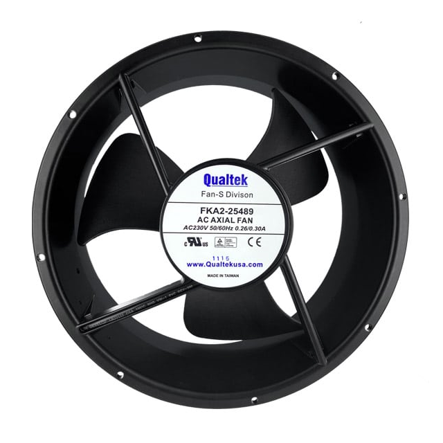
Qualtek Electronics Corporation
From $76.52 • 9 units available from DigiKey
KA225S
Qualtek Electronics Corporation
Fan Tubeaxial 115VAC Round - 254mm Dia Ball 630.0 CFM (17.64m³/min) 2 Terminals
| Distributor | SKU | Stock | MOQ | 1 | 10 | 50 | 100 | 1,000 | 10,000 | |
|---|---|---|---|---|---|---|---|---|---|---|
| DigiKey | Q607-ND | 9 | $94.46 | $84.89 | $78.31 | $76.52 | $76.52 | $76.52 | Buy |
EV-ADF4360-2EB1Z

Analog Devices Inc.
EV-ADF4360-2EB1Z
Analog Devices Inc.
The ADF4360-2 is a fully integrated integer-N synthesizerand voltage-controlled oscillator (VCO). The ADF4360-2 isdesigned for a center frequency of 2000 MHz. In addition, adivide-by-2 option is available, whereby the user gets an RFoutput of between 925 MHz and 1085 MHz.Control of all the on-chip registers is through a simple 3-wireinterface. The device operates with a power supply rangingfrom 3.0 V to 3.6 V and can be powered down when not in use.Applications Wireless handsets (DECT, GSM, PCS, DCS, WCDMA) Test equipment Wireless LANs CATV equipment
EV-ADUCRF101QS3Z

Analog Devices Inc.
EV-ADUCRF101QS3Z
Analog Devices Inc.
The ADuCRF101 is a fully integrated, data acquisition solution that is designed for low power, wireless applications. It features a 12-bit analog-to-digital converter (ADC), a low power ARM Cortex?-M3 processor, a 862 MHz to 928 MHz and 431 MHz to 464 MHz RF transceiver, and Flash?/EE memory. The ADuCRF101 is packaged in a 9 mm ? 9 mm LFCSP.The data acquisition section consists of a 12-bit SAR ADC. The six inputs can be configured in single-ended or differential mode. When configured in single-ended mode, they can be used for ratiometric measurements on sensors that are powered, when required, from the internal low dropout regulator (LDO). An internal battery monitor channel and an on-chip temperature sensor are also available.This wireless data acquisition system is designed to operate in battery-powered applications where low power is critical. The device can be configured in normal operating mode or different low power modes under direct program control. In flexi mode, any peripheral can wake up the device and operate it. In hibernate mode, the internal wake-up timer remains active. In shutdown mode, only an external interrupt can wake up the device.The ADuCRF101 integrates a low power ARM Cortex-M3 processor. It is a 32-bit RISC machine, offering up to 1.25 DMIPS peak performance. The ARM Cortex-M3 processor also has a flexible 14-channel direct memory access (DMA) controller that supports communication peripherals, serial peripheral interface (SPI), UART, and I2C. Also provided on chip are 128 kB of nonvolatile Flash/EE memory and 16 kB of SRAM.A 16 MHz on-chip oscillator generates the system clock. This clock can be internally divided for the processor to operate at a lower frequency, thus saving power. A low power, internal 32 kHz oscillator is available and can be used to clock the four timers, as follows: two general-purpose timers, a wake-up timer, and a system watchdog timer.A range of communication peripherals can be configured, as required, in a specific application. These peripherals include UART, I2C, SPI, GPIO ports, PWM, and RF transceivers.The RF transceiver communicates in the 862 MHz to 928 MHz and 431 MHz to 464 MHz frequency bands using multiple configurations.On-chip factory firmware supports in-circuit serial download via the UART, and nonintrusive emulation and program download are also supported via the serial wire interface. These features are incorporated into a low cost development system supporting this precision analog microcontroller family.The ADuCRF101 operates from 2.2 V to 3.6 V and is specified over an industrial temperature range of ?40?C to +85?C. It is available in a 64-lead LFCSP packageApplications Battery powered wireless sensor Medical telemetry systems Industrial and home automation Asset tracking Security systems (access systems) Health and fitness applications??

MSP430 Interface to the ADS1293 Code Library
Texas Instruments
MSP430 Interface to the ADS1293 Code Library
Texas Instruments
The MSP430 is an ideal microcontroller solution for low-cost low-power precision sensor applications because it consumes very little power. The ADS1293 is a fully integrated signal chain for portable low-power medical electrocardiogram (ECG) sports and fitness applications. This library provides functions to facilitate the interfacing of any MSP430 device to the ADS1293. An
Optimized automotive 1-megapixel camera module design for uncompressed digital video over coax

Texas Instruments
Optimized automotive 1-megapixel camera module design for uncompressed digital video over coax
Texas Instruments
The TIDA-00262 Reference Design is a high speed serial video interface to connect a remote automotive camera module to a display or machine vision processing system. It uses TIs FPD-Link III SerDes technology to transmit uncompressed MegaPixel video data: bidirectional control signals and power either over shielded twisted pair or coax cable.
EVAL-AD7403FMCZ

Analog Devices Inc.
EVAL-AD7403FMCZ
Analog Devices Inc.
The AD7403 is a high performance, second-order, ?-? modulator that converts an analog input signal into a high speed, single-bit data stream, with on-chip digital isolation based on Analog Devices, Inc., iCoupler? technology. The AD7403 operates from a 5 V (VDD1) power supply and accepts a differential input signal of ?250 mV (?320 mV full-scale). The differential input is ideally suited to shunt voltage monitoring in high voltage applications where galvanic isolation is required.The analog input is continuously sampled by a high performance analog modulator, and converted to a ones density digital output stream with a data rate of up to 20 MHz. The original information can be reconstructed with an appropriate digital filter to achieve 88 dB signal to noise ratio (SNR) at ?78.1 kSPS. The serial input/output can use a 5 V or a 3 V supply (VDD2).The serial interface is digitally isolated. High speed complementary metal oxide semiconductor (CMOS) technology, combined with monolithic transformer technology, means the on-chip isolation provides outstanding performance characteristics, superior to alternatives such as optocoupler devices. The AD7403 device is offered in a 16-lead, wide-body SOIC package and has an operating temperature range of ?40?C to +125?C. The AD7403-8 device is offered in an 8-lead, wide-body SOIC package and has an operating temperature range of ?40?C to +105?C.Applications Shunt current monitoring AC motor controls Power and solar inverters Wind turbine inverters Data acquisition systems Analog-to-digital and opto-isolator replacements
LT8644S | 8V, 16A Synchronous Step-Down Silent Switcher 2

Analog Devices Inc.
LT8644S | 8V, 16A Synchronous Step-Down Silent Switcher 2
Analog Devices Inc.
Demonstration circuit 2779A is an 8V, 16A synchronous step-down Silent Switcher® 2 with spread spectrum frequency modulation featuring the LT8644S. The demo board is designed for 1.2V output from a 2.7V to 8V input. The LT8644S is a compact, ultralow emission, high efficiency, and high speed synchronous monolithic stepdown switching regulator. The integrated bypass capacitors optimize all the fast current loops and make it easier to minimize EMI emissions by reducing layout sensitivity. Selectable spread spectrum mode further improves EMI performance, making it perfect solution to the noise sensitive applications. Peak current mode control with minimum on-time of as low as 20ns allows high step-down conversion even at high frequency. The LT8644S switching frequency can be programmed either via an external resistor or an external clock over a 300kHz to 3.5MHz range. The default frequency of demo circuit 2779A is 2MHz. The SYNC/MODE pin on the demo board DC2779A is grounded (JP1 at BURST position) by default for low ripple Burst Mode® operation. It can be configured into different operation modes through JP1 and SYNC terminal (Table 1 in the demo manual). Figure 4 in the demo manual shows the efficiency of the circuit at 3.3V input and 5V input in force continuous mode operation (input from VIN terminal). To get accurate efficiency measurement, measure the input voltage at the VIN_SENSE/GND terminals and measure the output voltage at the VOUT+ SENSE/VOUT– SENSE terminals. Figure 5 shows the LT8644S temperature rise on DC2779A demo board at 3.3V input and 5V input in forced continuous mode. The LT8644S is assembled in a 4mm × 4mm LQFN package with exposed pads for low thermal resistance. The rated maximum continuous load current is 16A, while derating may be necessary for certain input voltage and thermal conditions. The demo board has an EMI filter installed. This EMI filter can be included by applying the input voltage at the VEMI terminal. The EMI performance of the board (with EMI filter) is shown on Figure 6 in the demo manual. The red lines in EMI Performance are CISPR25 Class 5 limits. The figure shows that the LT8644S circuit passes the test with a wide margin. To achieve EMI performance as shown in Figure 6, the input EMI filter is required and the input voltage should be applied to VEMI terminal, and the test setup can be referred to the CISPR25 standards. If the input is applied to VIN terminal, the EMI filter is bypassed. The LT8644S data sheet gives a complete description of the part, the operation and application information. The data sheet must be read in conjunction with the demo manual for demo circuit 2779A. The layout recommendations for low EMI operation and maximum thermal performance are available in the data sheet section Low EMI PCB Layout and Thermal Considerations. Contact ADI applications engineer for support.
LTC3617EUDD Demo Board | VIN=2.25V to 5.5V, VOUT1 = 0.5VIN (VTT) @ ±6A, VOUT2 = 0.5VIN (VTTR) @ ±10mA

Analog Devices Inc.
LTC3617EUDD Demo Board | VIN=2.25V to 5.5V, VOUT1 = 0.5VIN (VTT) @ ±6A, VOUT2 = 0.5VIN (VTTR) @ ±10mA
Analog Devices Inc.
Demonstration circuit 1707 is a high efficiency monolithic step-down DC/DC switching regulator designed for double-data-rate (DDR) memory termination in computer systems. The VTT output is capable of sourcing and sinking up to 6A with an output voltage equal to one-half the voltage applied to the VDDQIN terminal or one-half the input supply voltage, selected by a jumper. An additional low current output (VTTR) also equal to one-half the voltage on VDDQIN can source and sink up to 10mA. Input voltage range is from 2.25V to 5.5V with overvoltage protection for transients exceeding 6.5V.


Sensorless Trapezoidal Control of BLDC Motors (Rev. A)
Texas Instruments
Sensorless Trapezoidal Control of BLDC Motors (Rev. A)
Texas Instruments
This application report presents a solution for the control of brushless DC motors using theTMS320F2803x microcontrollers. TMS320F280x devices are part of the C2000™ family ofmicrocontrollers that enable the cost-effective design of intelligent controllers for three-phase motors byreducing the system components and increasing efficiency. Using these devices it is possible to realizefar mo