
Search results

EVAL-AD7843EBZ

Analog Devices Inc.
EVAL-AD7843EBZ
Analog Devices Inc.
The AD7843 is a 12-bit successive-approximation ADC with a synchronous serial interface and low on resistance switches for driving touch screens. The part operates from a single 2.2 V to 5.25 V power supply and features throughput rates greater than 125 kSPS. The external reference applied to the AD7843 can be varied from 1 V to +VCC, while the analog input range is from 0 V to VREF. The device includes a shutdown mode that reduces the current consumption to less than 1 ?A. This part is available in a 16-lead 0.15' Quarter Size Outline (QSOP) package and a 16-lead Thin Shrink Small Outline (TSSOP) package.?Also see the AD7843 sister part, which is the AD7873. This part is similar to the AD7843 but has added functionality such as an on-chip temperature sensor (-40?C to + 85?C), on-chip 2.5 V reference and direct battery and touch-pressure measurement.
CC1120EM 955 MHz Reference Design

Texas Instruments
CC1120EM 955 MHz Reference Design
Texas Instruments
The CC1120 955MHz EM reference design contains schematics and layout files for the CC1120EM 955MHz evaluation module. The reference design demonstrates good techniques for CC1120 decoupling and RF layout. For optimum RF performance: these parts should be copied accurately. This is a 4-layer reference design with a discrete balun and an SMA antenna connector designed for a single ended 50 ohm antenna. The RF section has been designed and characterized for operation in the 955 MHz frequency band.
Interfacing the TLC5510 Analog-to-Digital Converter to the TMS320C203 DSP
Texas Instruments
Interfacing the TLC5510 Analog-to-Digital Converter to the TMS320C203 DSP
Texas Instruments
This application report presents guidelines for interfacing the Texas Instruments (TI(TM)) TLC5510 8-bit parallel-output analog-to-digital converter (ADC) to the TI TMS320C203 DSP data bus. The 8-bit ADC operates at a rate of 20 MHz. The C callable application program (assembly code) used to initialize the TMS320C203 and execute the code is also discussed.This report serves as reference inform
JESD204B Link Latency Design Using a High Speed ADC

Texas Instruments
JESD204B Link Latency Design Using a High Speed ADC
Texas Instruments
JESD204B links are the latest trend in data-converter digital interfaces. These links take advantage of high-speed serial-digital technology to offer many compelling benefits including improved channel densities. This reference design addresses one of the challenges of adopting the new interface: understanding and designing the link latency. An example achieves deterministic latency and determines the link latency of a system containing the Texas Instruments LM97937 ADC and Xilinx Kintex 7 FPGA.
12-mm Tape-and-Reel Component-Delivery System
Texas Instruments
12-mm Tape-and-Reel Component-Delivery System
Texas Instruments
The design advances of component pick-and-place automated equipment for board assembly increasingly are pushing the margins of the tape-and-reel packing configurations. The continuing drive for faster assembly reduces the index time and tends to amplify the forces acting on the tape-and-reel component-delivery system. The magnified forces when combined with a high carrier-tape width-to-component
AD9517-3A/PCBZ

Analog Devices Inc.
AD9517-3A/PCBZ
Analog Devices Inc.
The AD9517-31 provides a multi-output clock distribution function with subpicosecond jitter performance, along with an on-chip PLL and VCO. The on-chip VCO tunes from 1.75 GHz to 2.25 GHz. Optionally, an external VCO/VCXO of up to 2.4 GHz can be used.The AD9517-3 emphasizes low jitter and phase noise to maximize data converter performance, and it can benefit other applications with demanding phase noise and jitter requirements.The AD9517-3 features four LVPECL outputs (in two pairs) and four LVDS outputs (in two pairs). Each LVDS output can be reconfigured as two CMOS outputs. The LVPECL outputs operate to 1.6 GHz, the LVDS outputs operate to 800 MHz, and the CMOS outputs operate to 250 MHz.For applications that require additional outputs, a crystal reference input, zero-delay, or EEPROM for automatic configuration at startup, the AD9520 and AD9522 are available. In addition, the AD9516 and AD9518 are similar to the AD9517 but have a different combination of outputs.Each pair of outputs has dividers that allow both the divide ratio and coarse delay (or phase) to be set. The range of division for the LVPECL outputs is 1 to 32. The LVDS/CMOS outputs allow a range of divisions up to a maximum of 1024.The AD9517-3 is available in a 48-lead LFCSP and can be operated from a single 3.3 V supply. An external VCO, which requires an extended voltage range, can be accommodated by connecting the charge pump supply (VCP) to 5 V. A separate LVPECL power supply can be from 2.5 V to 3.3 V (nominal).The AD9517-3 is specified for operation over the industrial range of ?40?C to +85?C.APPLICATIONS Low jitter, low phase noise clock distribution 10/40/100 Gb/sec networking line cards, including SONET, Synchronous Ethernet, OTU2/3/4 Forward error correction (G.710) Clocking high speed ADCs, DACs, DDSs, DDCs, DUCs, MxFEs High performance wireless transceivers ATE and high performance instrumentation 1 AD9517 is used throughout to refer to all the members of the AD9517 family. However, when AD9517-3 is used, it is referring to that specific member of the AD9517 family.

LTC3535EDD Demo Board | Dual Channel 550mA 1MHz Synchronous Step-Up DC/DC Converter

Analog Devices Inc.
LTC3535EDD Demo Board | Dual Channel 550mA 1MHz Synchronous Step-Up DC/DC Converter
Analog Devices Inc.
DC1483A: Demo Board for the LTC3535 Dual Channel 550mA 1MHz Synchronous Step-Up DC/DC Converter.

DC1928A

Analog Devices Inc.
DC1928A
Analog Devices Inc.
The LTC3867 is a current mode synchronous step-down switching regulator controller that drives all N-channel power MOSFET stages. Output voltage transient excursions are minimized by use of a nonlinear control architecture to eliminate clock latency issues.The maximum current sense voltage is programmable from 30mV to 75mV, allowing the use of either a discrete sense resistor or the inductor DCR as the sensing element. Programmable DCR temperature compensation allows constant current limit regardless of inductor temperature. Programmable inductor temperature-based thermal shutdown protects the power components from thermal stress. Soft recovery from output shorts or overcurrent minimizes output overshoot.The LTC3867 features a precision 0.6V reference and can regulate output voltages up to 14V from a wide 4V to 38V input supply range. The LTC3867 includes a high speed differential remote sense amplifier. Burst Mode? operation, continuous and pulse-skipping modes are supported. The LTC3867 is available in a 24-lead (4mm ? 4mm) QFN package.Applications Automotive Systems Telecom Systems Industrial Equipment Distributed DC Power Systems

131384-HMC1010LP4E

Analog Devices Inc.
131384-HMC1010LP4E
Analog Devices Inc.
The HMC1010LP4E Power Detector is designed for RF power measurement, and control applications for frequencies up to 3.9 GHz. The detector provides an accurate RMS representation of any RF/IF input signal. The output is a temperature compensated monotonic, representation of real signal power, measured with an input sensing range of 60 dB.The HMC1010LP4E is ideally suited to those wide bandwidth, wide dynamic range applications, requiring repeatable measurement of real signal power, especially where RF/IF wave shape and/or crest factor change with time.The integration bandwidth of the HMC1010LP4E is digitally programmable with the use of input pins SC I1- 4 with a range of more than 4 decades. This allows the user to dynamically set the operation bandwidth providing the capability of handling different types of modulations on the same platform.The HMC1010LP4E features an internal op-amp at output stage, which provides for slope & intercept adjustments and enables controller application.Applications Log ?> Root-Mean-Square?(RMS) Conversion Received Signal Strength?Indication (RSSI) Transmitter Signal Strength?Indication (TSSI) RF Power Amplifier Efficiency Control Receiver Automatic Gain Control Transmitter Power Control
Primary-Side Regulated Flyback for Universal AC Input and 15V/0.25A Output Reference Design

Texas Instruments
Primary-Side Regulated Flyback for Universal AC Input and 15V/0.25A Output Reference Design
Texas Instruments
The PMP9171 reference design uses the UCC28910 primary-side regulated flyback controller with integrated MOSFET to generate a 15V/0.25A output from an univeral AC input with safety isolation rated transformer. 80% efficiency is achieved at full load and less than 130mW power consumption is observed during no load condition.
SEPIC (5V@250mA) for Auxiliary Bias Supply

Texas Instruments
SEPIC (5V@250mA) for Auxiliary Bias Supply
Texas Instruments
The PMP5298 reference design provides an isolated 5V at 250mA from a 120VAC/60Hz input in less than 1 square inch of board space. This design uses the UCC3813-5 in a non-isolated SEPIC topology. The SEPIC clamping capacitor reduces ringing on the drain of the MOSFET and recaptures leakage energy to improve efficiency.
Automotive 200-VA High Frequency Inverter Design
Texas Instruments
Automotive 200-VA High Frequency Inverter Design
Texas Instruments
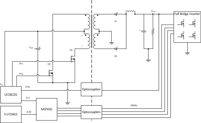
This design presents a low-cost: small size: robust 200-VA DC to AC inverter based on TI’s MSP430 and UCD8220-digitally managed push-pull controller. It is targetted towards car inverters and small-segment inverters for commercial applications. In this design: UCD8220 is used for a boost stage to get 250-V DC from a 12-V battery. The MSP430 acts as a host controller and provides a 100-kHz clock to UCD8220 and drives for output DC-AC bridge. This inverter has a peak efficiency of 90% and has natural cooling and does not require a fan for cooling.