
Search results
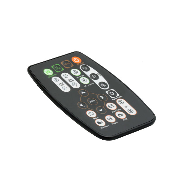
LTC4234 Demo Board | 20A Guaranteed SOA Hot Swap Controller

Analog Devices Inc.
LTC4234 Demo Board | 20A Guaranteed SOA Hot Swap Controller
Analog Devices Inc.
Demonstration circuit 2116A features the LTC4233/LTC4234 10A/20A Guaranteed SOA Hot Swap™ Controllers. The LTC4233 and LTC4234 are ideally suited for compact power distribution control in 2.9V to 15V applications for hot board insertion protection, high side power switching, and electronic circuit breaker functions.
Integrated Gate Driver for Residential Inverters Reference Design

Texas Instruments
Integrated Gate Driver for Residential Inverters Reference Design
Texas Instruments
The PMP9455 reference design provides a highly integrated gate driver solution for 800VA to 3kVA iPure Sine Wave Low Frequency Inverter application . With its unique features of higher peak current drive capability along with integration of two transconductance amplifier with external programmable gain and filtering : the design is a perfect fit for industrial applications . The daughter card design of SM72295 can also be used in various other four switch power topologies such as Buck Boost: Interleaved Buck etc. The Reference design has also been successfully tested on Solar MPPT charger : the details of which can also be found in TIDA-00120 design (http://www.ti.com/tool/TIDA-00120).
24VDC 10A eFuse and Protection Circuit for Programmable Logic Controllers (PLC)

Texas Instruments
24VDC 10A eFuse and Protection Circuit for Programmable Logic Controllers (PLC)
Texas Instruments
This sub system design shows an IC based implementation of over voltage: over current: reverse current: reverse polarity and miss wire protection which is more accurate: lower power and faster compared to fuses: PTCs and diodes. Programmable Logic Controller (PLC) I/O modules connected to a field power supply benefit from protection on the 24V field input connectors as power supply faults or miss wiring might damage or cause the module to not operate correctly.

EVAL01-HMC987LP5E

Analog Devices Inc.
EVAL01-HMC987LP5E
Analog Devices Inc.
The HMC987LP5E 1-to-9 fanout buffer is designed for low noise clock distribution. It is intended to generate relatively square wave outputs with rise/fall times < 100 ps. The low skew and jitter outputs of the HMC987LP5E, combined with its fast rise/fall times, leads to controllable low-noise switching of downstream circuits such as mixers, ADCs/DACs or SERDES devices. The noise floor is particularly important in these applications, when the clocknetwork bandwidth is wide enough to allow squarewave switching. Driven at 2 GHz, outputs of the HMC987LP5E have a noise floor of ?166 dBc/Hz, corresponding to a jitter density of 0.6 asec/rtHz - or 50 fs over an 8 GHz bandwidth.The input stage can be driven single-ended or differentially, in a variety of signal formats (CML, LVDS, LVPECL or CMOS), AC or DC coupled. The input stage also features adjustable input impedance. It has 8 LVPECL outputs, and 1 CML output with adjustable swing/power-level in 3 dB steps.Individual output stages may be enabled or disabled for power-savings when not required using either hardware control pins, or under control of a serial-port interface.APPLICATIONS SONET, Fibre Channel,?GigE Clock Distribution ADC/DAC Clock Distribution Low Skew and Jitter Clock?or Data Fanout Wireless/Wired Communications Level Translation High Performance Instrumentation Medical Imaging Single-Ended to Differential?Conversion
RC0805FR-1356K2L

Yageo
From $0.00 • 100 k+ units available from multiple sources
RC0805FR-1356K2L
Yageo
Res Thick Film 0805 56.2K Ohm 1% 1/8W ±100ppm/°C Molded SMD SMD Paper T/R
| Distributor | SKU | Stock | MOQ | 1 | 10 | 50 | 100 | 1,000 | 10,000 | |
|---|---|---|---|---|---|---|---|---|---|---|
| DigiKey | 13-RC0805FR-1356K2LCT-ND | 39,837 | 1 | $0.10 | $0.01 | $0.01 | $0.01 | $0.01 | $0.01 | Buy |
| Mouser Electronics | 603-RC0805FR-1356K2L | 54,275 | 1 | $0.10 | $0.02 | $0.02 | $0.01 | $0.01 | $0.01 | |
| AVNET Express | RC0805FR-1356K2L | 0 | 20,000 | Buy | ||||||
| AVNET Europe | RC0805FR-1356K2L | 0 | 20,000 | Buy | ||||||
| Arrow North American Components | RC0805FR-1356K2L | 0 | 20,000 | |||||||
| Quarktwin Electronic Components | RC0805FR-1356K2L | 23,430 | 10 | $0.00 | $0.00 | $0.00 | $0.00 | $0.00 | $0.00 | Buy |
6 to 16Vin 12V@4A Output Wide Vin SEPIC Converter Reference Design

Texas Instruments
6 to 16Vin 12V@4A Output Wide Vin SEPIC Converter Reference Design
Texas Instruments
This is a Wide-Vin SEPIC converter with an operating input voltage range of 6V to 16V: and implements an output of 12V with the capability of supplying 4A of current to load.
EVAL-AD5677RSDZ
Analog Devices Inc.
EVAL-AD5677RSDZ
Analog Devices Inc.
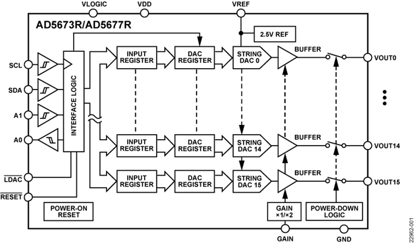
The AD5673R/AD5677R are low power, 16-channel, 12-/16-bit, buffered voltage output, digital-to-analog converters (DACs) that include a 2.5 V, 2 ppm/?C internal reference (enabled by default), and a gain select pin, resulting in a full-scale output of 2.5 V (gain = 1) or 5 V (gain = 2). The devices operate from a single, 2.7 V to 5.5 V supply range and are guaranteed monotonic by design. The AD5673R/AD5677R are available in a 28-lead lead frame chip scale package (LFCSP) and incorporate a power-on reset (POR) circuit that ensures that the DAC outputs power up to and remain at zero scale or midscale until a valid write. The AD5673R/AD5677R contain a power-down mode that reduces the current consumption to 2 ?A typical.Applications Optical transceivers Base station power amplifiers Process control (programmable logic controller (PLC) input/output cards) Industrial automation Data acquisition systems Product Highlights High channel density: 16 channels in 4 mm ? 4 mm LFCSP. High relative accuracy (INL). AD5673R (12-bit): ?1 LSB maximum. AD5677R (16-bit): ?4 LSB maximum. Low drift, 2.5 V, on-chip reference.
PFC Flyback LED Converter 40V - 120V @ 0.35A
Texas Instruments
PFC Flyback LED Converter 40V - 120V @ 0.35A
Texas Instruments
This active power factor correction: transition mode: isolated flyback generates a constant current of 350mA on an LED string from high line (180 to 264Vac). The output accepts a voltage range of 40 to 120V. Open LED protection (overvoltage) and safety discharge of output capacitors are implemented as well.
EVAL-ADAQ4001FMCZ

Analog Devices Inc.
EVAL-ADAQ4001FMCZ
Analog Devices Inc.
The ADAQ4001 is a ?Module? precision data acquisition (DAQ), signal chain solution that reduces the development cycle of a precision measurement system by transferring the signal chain design challenge of component selection, optimization, and layout from the designer to the device. Using system-in-package (SIP) technology, the ADAQ4001 reduces end system component count by combining multiple common signal processing and conditioning blocks into a single device. These blocks include a high resolution 16-bit, 2 MSPS successive approximation register (SAR), analog-to-digital converter (ADC), a low noise, fully differential ADC driver amplifier (FDA), and a stable reference buffer. Using Analog Devices, Inc., iPassives? technology, the ADAQ4001 also incorporates crucial passive components with superior matching and drift characteristics to minimize temperature dependent error sources and to offer optimized performance (see Figure 1 in the data sheet). Housing this signal chain solution in a small, 7 mm ? 7 mm, 0.80 mm pitch, 49-ball CSP_BGA enables compact form factor designs without sacrificing performance and simplifies end system bill of materials management. This level of system integration makes the ADAQ4001 much less sensitive to printed circuit board (PCB) layout while still providing flexibility to adapt to a wide range of signal levels. The serial peripheral interface (SPI)-compatible, serial user interface is compatible with 1.8 V, 2.5 V, 3 V, or 5 V logic, using a separate VIO supply. Specified operation of the ADAQ4001 is from ?40?C to +125?C.APPLICATIONSAutomatic test equipmentMachine automationProcess controlsMedical instrumentationDigital control loops
EVAL-ADAU1472Z

Analog Devices Inc.
EVAL-ADAU1472Z
Analog Devices Inc.
The ADAU1472 is a high quality SigmaDSP? digital audio?processor with a large internal memory, enabling efficient audio?source separation, far field voice capture, speech processing, deep?learning, and advanced audio signal processing. The processor combines the highly optimized Cadence? Tensilica? HiFi? 4?audio/voice processor with custom Analog Devices, Inc.,?instruction extensions for math acceleration, and a flexible input and output architecture. The?HiFi 4 processor supports four 32-bit ? 32-bit multiplier?accumulators (MACs) per cycle with 72-bit accumulators, dual 64-bit memory load, and a native Institute of Electrical and?Electronics Engineers (IEEE) single precision, floating-point multiplier.The ADAU1472 processor offers performance up to 270.336 MHz,?supports low latency, sample by sample audio processing, and?block by block processing paradigms in parallel. The integer?phase-locked loop (PLL) and flexible clock generator hardware?can generate up to 15 audio sample rates simultaneously (8 kHz?to 192 kHz). These clock generators, along with the on-board?asynchronous sample rate converters (ASRCs) and flexible?hardware audio routing matrix, greatly simplify the design of?complex audio systems.The HiFi 4 digital signal processor (DSP) core has 480 kB of L1?memory running at the DSP core clock rate, which consists of?256 kB data random access memory (RAM), 64 kB instruction?RAM, 128 kB data cache, and 32 kB instruction cache, along with?2 MB of L2 system static random access memory (SRAM)?running at one half of the DSP core clock rate. The processor?also supports up to 2 GB of external flash memory to enable the?storage of large data tables and self boot code.Dual on-chip power domains allow low power operation,?including the capability of routing audio through a flexible audio?routing matrix with IOVDD as the only active supply.?The configurable voice detection hardware can detect human?speech onset while operating in a low power state and can?generate both internal DSP and external wake-up signals.The ADAU1472 interfaces with a wide range of analog-to-digital?converters (ADCs), digital-to-analog converters (DACs), digital?audio devices, amplifiers, and control circuitry due to its highly?configurable serial ports, Sony/Philips digital interface?format (S/PDIF) interfaces, and multipurpose input/output?pins. The device can also directly interface with up to 14 pulse?density modulated (PDM) output microphones due to?integrated decimation filters specifically designed for that?purpose. The PDM outputs with integrated interpolation filters?provide direct connectivity to PDM input Class D amplifiers.The processor has two serial peripheral interface (SPI) bus master?control ports that allow the device to communicate with multiple?SPI-compatible devices including support for single, dual, and?quad input/output operation. In addition, the SPI flash port?allows direct memory mapped read access with minimal central?processing unit (CPU) overhead and standalone self boot?operation.The combined high performance DSP core, large RAM, and?small footprint make the ADAU1472 an ideal replacement for?large, general-purpose DSPs that consume more power for the?same processing load.Applications Far field voice interface devices Audio source separation Embedded deep learning for audio Commercial and professional audio processing
Cost-Effective Transformerless Offline Supply for Light Load Applications (Rev. A)

Texas Instruments
Cost-Effective Transformerless Offline Supply for Light Load Applications (Rev. A)
Texas Instruments
This design idea provides a simple non-isolated AC/DC power supply for low power applications. Thedesign uses a capacitive-dropper front-end combined with a LM46000 SIMPLE SWITCHER® buckregulator from Texas Instruments. The circuit provides 3.3 V at a minimum of 100 mA from a line supply of90 VAC to 265 VAC. Theory of operation as well as design equations and performance results are given.
Standalone Synchronous Switch-mode Li-Ion Charger with 2A FET Reference Design

Texas Instruments
Standalone Synchronous Switch-mode Li-Ion Charger with 2A FET Reference Design
Texas Instruments
This reference design is a solution for a Li-Ion charge management IC. It has a highly integrated battery charge IC utilizing synchronous switch mode power conversion for efficient and comprehensive charge control of a single cell Li-Ion battery. The solutionprovides a convenient method to evaluate the operation and performance of the IC.
36V-72Vdc Input: 12V/200W Active Clamp Forward - Reference Design

Texas Instruments
36V-72Vdc Input: 12V/200W Active Clamp Forward - Reference Design
Texas Instruments
This reference design generates a 12V/16A output from a standard 48V DC telecom input. The UCC2897A controls an active clamp forward converter power stage. The low gate charge and low RDSon of the CSD19533Q51: implemented as self-driven synchronous rectifiers: allow this design to achieve a peak efficiency of 95%. The compact UCC27511 drivers simplify the gate drive circuitry for the synchronous rectifiers.