
Search results
AD7134 Evaluation Board
Analog Devices Inc.
AD7134 Evaluation Board
Analog Devices Inc.
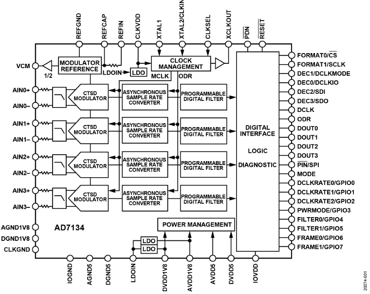
The EVAL-AD7134FMCZ evaluation kit features the AD7134 24-bit, 4-channel, simultaneous sampling, 1.5 MSPS precision alias free analog-to-digital converter (ADC). Two on-board AD7134 ADCs are included to demonstrate multidevice simultaneous sampling. The EVAL-AD7134FMCZ draws power from the system demonstration platform (SDP) EVAL-SDP-CH1Z (SDP-H1) board, and the on-board dc-to-dc regulators regulate an external supply of 8 V to 14 V down to 5 V, 1.8 V, and 1.2 V to supply the AD7134 and peripheral components. Both on-board ADCs have a separate reference of 4.096 V generated by the on-board ADR444. The ADCs have three clock input options and can be clocked by a crystal input, a microelectromechanical system (MEMS) oscillator, or a complementary metal-oxide semiconductor (CMOS) clock. The EVAL-AD7134FMCZ connects to the PC USB port via the SDP-H1 board. The AD7134 evaluation software running on a PC provides full accessibility to the AD7134 device register map, as well as a data analysis interface to display key parameters and graphics from the conversion result in both time and frequency domains. For full details on the AD7134, see the AD7134 data sheet, which must be consulted in conjunction with this user guide when using the EVAL-AD7134FMCZ.
ADP2138CB-1.0EVALZ

Analog Devices Inc.
ADP2138CB-1.0EVALZ
Analog Devices Inc.
The ADP2138 and ADP2139 are high efficiency, low quiescent current, synchronous step-down dc-to-dc converters. The ADP2139 has the additional feature of an internal discharge switch. The total solution requires only three tiny external components. When the MODE pin is set high, the buck regulator operates in forced PWM mode, which provides low peak-to-peak ripple for power supply noise sensitive loads at the expense of light load efficiency. When the MODE pin is set low, the buck regulator automatically switches operating modes, depending on the load current level. At higher output loads, the buck regulator operates in PWM mode. When the load current falls below a predefined threshold, the regulator operates in power save mode (PSM), improving light load efficiency.The ADP2138/ADP2139 operate on input voltages of 2.3 V to 5.5 V, which allows for single lithium or lithium polymer cell, multiple alkaline or NiMH cell, PCMCIA, USB, and other standard power sources. The maximum load current of 800 mA is achievable across the input voltage range.The ADP2138/ADP2139 are available in fixed output voltages of 3.3 V, 3.0 V, 2.8 V, 2.5 V, 1.8 V, 1.5 V, 1.2 V, 1.0 V, and 0.8 V. All versions include an internal power switch and synchronous rectifier for minimal external part count and high efficiency. The ADP2138/ADP2139 have internal soft start and they are internally compensated. During logic controlled shutdown, the input is disconnected from the output and the ADP2138/ADP2139 draw 0.2 ?A (typical) from the input source.Other key features include undervoltage lockout to prevent deep battery discharge, and soft start to prevent input current overshoot at startup. The ADP2138/ADP2139 are available in a 6-ball wafer level chip scale package (WLCSP).Applications PDAs and palmtop computers Wireless handsets Digital audio, portable media players Digital cameras, GPS navigation units
ADL5390-EVALZ

Analog Devices Inc.
ADL5390-EVALZ
Analog Devices Inc.
The ADL5390 vector multiplier consists of a matched pair of broadband variable gain amplifiers whose outputs are summed. The separate gain controls for each amplifier are linear-in-magnitude. If the two input RF signals are in quadrature, the vector multiplier can be configured as a vector modulator or as a variable attenuator/phase shifter by using the gain control pins as Cartesian variables. In this case, the output amplitude can be controlled from a maximum of +5 dB to less than -30 dB, and the phase can be shifted continuously over the entire 360? range. Since the signal paths are linear, the original modulation on the inputs is preserved. If the two signals are independent, then the vector multiplier can function as a 2:1 multiplexer or can provide fading from one channel to another.The ADL5390 operates over a wide frequency range of 20 MHz to 2400 MHz. For a maximum gain setting on one channel at 380 MHz, the ADL5390 delivers an OP1dB of 11 dBm, an OIP3 of 24 dBm, and an output noise floor of -148 dBm/Hz. The gain and phase matching between the two VGAs is better than 0.5 dB and 1?, respectively, over most of the operating range.The ADL5390 is fabricated on Analog Devices' proprietary, high performance 25 GHz SOI complementary bipolar IC process. It is available in a 24-lead, Pb-free CSP package and operates over a -40?C to +85?C temperature range. Evaluation boards are available.APPLICATIONS PA linearization and predistortion Amplitude and phase modulation Variable matched attenuator and/or phase shifter Cellular base stations Radio links Fixed wireless access Broadband/CATV RF/IF analog multiplexerAVAILABILITYSamples, part number ADL5390ACPZ, and an evaluation board, part number ADL5390-EVAL, are available.COMPANION PRODUCTSAD8302 - LF to 2.7GHz RF/IF Gain Phase DetectorAD8340 - RF Vector Modulator 700MHz to 1000MHzAD8341 - RF Vector Modulator 1.5GHz to 2.4GHz
Analog Front End for Motor Electronic Overload Relays with Enhanced Current Range

Texas Instruments
Analog Front End for Motor Electronic Overload Relays with Enhanced Current Range
Texas Instruments
This reference design is the analog front end (AFE) for an electronic overload relay: used for monitoring and protecting motors from overcurrent or undercurrent events. It is an ideal tool for developers creating overload relays for sensitive AC motors in industrial applications. This programmable gain amplifier (PGA) based analog front end is intended to be an easy evaluation platform for an accurate: industry-leading 10:1 full load ampere (FLA) range and is repeatable over a -10 to +70 °C temperature range.
36V-72VDC Input Active Clamp Forward With Dual 12V/50W Outputs

Texas Instruments
36V-72VDC Input Active Clamp Forward With Dual 12V/50W Outputs
Texas Instruments
This power supply design generates a 12V/100W isolated output from a standard 48V telecom input. An active clamp forward converter is controlled by the UCC2897A. The INA202 and an external PFET are used to provide a current limited 12V/4.5A output derived from the main 12V output of the forward converter. This power supply has a peak efficiency of over 94%.
Tiny Wireless Receiver for Low Power Wearable Applications Reference Design

Texas Instruments
Tiny Wireless Receiver for Low Power Wearable Applications Reference Design
Texas Instruments
TI design TIDA-00329 is suitable for low power wearable devices and incorporates a wireless power receiver (bq51003) or a wireless power charger (bq51050B/51B). It features an ultra-small size (5.23 mm x 5.48 mm) and is capable of up to 2-W power delivery. The included schematic illustrates that all 3 devices can be implemented with a single design.
Security Tracker in Automotive Applications

Texas Instruments
Security Tracker in Automotive Applications
Texas Instruments
This reference design supports the supply for a security tracker using the TPS40200-Q1: with the opportunity of a wide input voltage range from 8V-50V. The output can handle 4.3V up to 3A due to the non-synchronous buck controller. The reference design also allows for flexible design with a simple configuration due to the device.
Small and Simple Isolated Flyback Universal Vin: 5.2V@200mA: Primary-side Regulated Reference Design

Texas Instruments
Small and Simple Isolated Flyback Universal Vin: 5.2V@200mA: Primary-side Regulated Reference Design
Texas Instruments
Design features low component count and low cost isolated flyback: converting the universal mains (85Vac…275Vac) to 5.2V@200mA. Due to primary side regulation of the controller UCC28700: no optocoupler is needed to close the loop.
TMS320C24x PWM Full Compare in Symmetric Mode

Texas Instruments
TMS320C24x PWM Full Compare in Symmetric Mode
Texas Instruments
There are three Full Compare Units in the Event Manager Module. Each Full Compare Unit has two associated PWM outputs. The time base for Full Compare Units is provided by GP Timer One.This application report presents applications of the Full Compare: up to six PWM three PWM plus three complemented PWM generation in symmetric mode.
ADP2140CPZ-REDYKIT

Analog Devices Inc.
ADP2140CPZ-REDYKIT
Analog Devices Inc.
The ADP2140 includes a high efficiency, low quiescent 600 mAstepdown dc-to-dc converter and a 300 mA LDO packaged in asmall 10-lead 3 mm ? 3 mm LFCSP. The total solution requiresonly four tiny external components.The buck regulator uses a proprietary high speed current-mode,constant frequency, pulse-width modulation (PWM) controlscheme for excellent stability and transient response. To ensurethe longest battery life in portable applications, the ADP2140 hasa power saving variable frequency mode to reduce switching frequencyunder light loads.The LDO is a low quiescent current, low dropout linear regulatordesigned to operate in a split supply mode with VIN2 as low as1.65 V. The low input voltage minimum allows the LDO to bepowered from the output of the buck regulator increasing efficiencyand reducing power dissipation. The ADP2140 runs frominput voltages of 2.3 V to 5.5 V allowing single Li+/Li? polymer cell, multiple alkaline/NiMH cell, PCMCIA, and other standardpower sources.ADP2140 includes a power-good pin, soft start, and internal?compensation. Numerous power sequencing options are user-selectable through two enable inputs. In autosequencing mode, the highest voltage output enables on the rising edge of EN1.?During logic controlled shutdown, the input disconnects from the output and draws less than 300 nA from the input source.?Other key features include: undervoltage lockout to prevent deep?battery discharge, soft start to prevent input current overshoot?at startup, and both short-circuit protection and thermal overload protection circuits to prevent damage in adverse conditions.When the ADP2140 is used with two 0603 capacitors, one 0402capacitor, one 0402 resistor, and one 0805 chip inductor, the totalsolution size is approximately 90 mm2 resulting in the smallest footprintsolution to meet a variety of portable applications.Applications Mobile phones Personal media players Digital camera and audio devices Portable and battery-powered equipment
ADP121CB-1.5-EVALZ

Analog Devices Inc.
ADP121CB-1.5-EVALZ
Analog Devices Inc.
The ADP121 is a quiescent current, low dropout, linear regulator that operates from 2.3 V to 5.5 V and provides up to 150 mA of output current. The low 135 mV dropout voltage at 150 mA load improves efficiency and allows operation over a wide input voltage range. The low 30 ?A of quiescent current at full load makes the ADP121 ideal for battery-operated portable equipment.The ADP121 is available in output voltages ranging from 1.2 V to 3.3 V. The parts are optimized for stable operation with small 1 ?F ceramic output capacitors. The ADP121 delivers good transient performance with minimal board area.Short-circuit protection and thermal overload protection circuits prevent damage in adverse conditions. The ADP121 is available in a tiny 5-lead TSOT and 4-ball 0.4 mm pitch WLCSP pack-ages and utilizes the smallest footprint solution to meet a variety of portable applications.