
Search results
Using Advanced Event Triggering to Debug Real-Time Problems in Embedded Systems

Texas Instruments
Using Advanced Event Triggering to Debug Real-Time Problems in Embedded Systems
Texas Instruments
As more and more system components become embedded within the system processor chip new techniques are required for debug. Signals and busses that were historically available for probe connection at external package pins are now hidden from the users within the processor package. This problem is referred to as vanishing visibility meaning that the user can no longer employ traditional techniques
W25Q64JVZEIQ-TR

Winbond Electronics Corporation
From $1.35 • 1 k+ units available from multiple sources
W25Q64JVZEIQ-TR
Winbond Electronics Corporation
SERIAL FLASH MEMORY 64M
| Distributor | SKU | Stock | MOQ | 1 | 10 | 50 | 100 | 1,000 | 10,000 | |
|---|---|---|---|---|---|---|---|---|---|---|
| DigiKey | 256-W25Q64JVZEIQTRDKR-ND | 2,982 | $1.11 | $1.04 | $0.99 | $0.97 | $0.89 | $0.85 | Buy | |
| AVNET Asia Pacific | W25Q64JVZEIQ-TR | 20,000 | 4,000 | Buy | ||||||
| Arrow North American Components | W25Q64JVZEIQ TR | 0 | 4,000 | $0.83 | ||||||
| Verical Marketplace | W25Q64JVZEIQ TR | 3,999 | 8 | $1.29 | $1.28 | $1.12 | $1.03 | $1.35 |
Working With Boost Converters
Texas Instruments
Working With Boost Converters
Texas Instruments
This brief note highlights some of the more common pitfalls when using boost regulators. These includemaximum achievable output current and voltage short circuit behavior and basic layout issues. It isassumed that the reader is familiar with the basic operation of a boost regulator.
Using GCC/GDB With SimpleLink CC26xx
Texas Instruments
Using GCC/GDB With SimpleLink CC26xx
Texas Instruments
This application report describes how to set up an open source software-based development environment for the SimpleLink CC26xx and CC13xx wireless MCUs using Eclipse as integrated development environment (IDE).
DC1908A-F
Analog Devices Inc.
DC1908A-F
Analog Devices Inc.
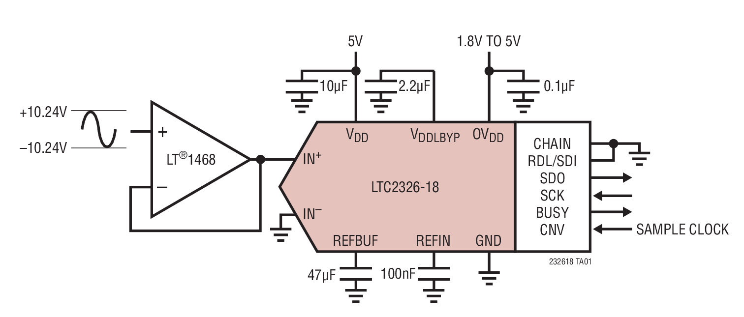
The LTC2326-18 is a low noise, high speed 18-bit successive approximation register (SAR) ADC with pseudo-differential inputs. Operating from a single 5V supply, the LTC2326-18 has a ?10.24V true bipolar input range, making it ideal for high voltage applications which require a wide dynamic range. The LTC2326-18 achieves ?5LSB INL maximum, no missing codes at 18 bits with 95dB SNR.The LTC2326-18 has an onboard single-shot capable reference buffer and low drift (20ppm/?C max) 2.048V temperature compensated reference. The LTC2326-18 also has a high speed SPI-compatible serial interface that supports 1.8V, 2.5V, 3.3V and 5V logic while also featuring a daisy-chain mode. The fast 250ksps throughput with no cycle latency makes the LTC2326-18 ideally suited for a wide variety of high speed applications. An internal oscillator sets the conversion time, easing external timing considerations. The LTC2326-18 dissipates only 28mW and automatically naps between conversions, leading to reduced power dissipation that scales with the sampling rate. A sleep mode is also provided to reduce the power consumption of the LTC2326-18 to 300?W for further power savings during inactive periods. Bits LTC2326-16 16 LTC2326-18 18 Applications Programmable Logic Controllers Industrial Process Control High Speed Data Acquisition Portable or Compact Instrumentation ATE
LTC3853EUJ Demo Board | Triple, PolyPhase, 6.5V ≤ VIN ≤ 14V, VOUT1 = 1.8V/15A, VOUT2 = 1.2V/15A, VOUT3 = 2.5V/15A

Analog Devices Inc.
LTC3853EUJ Demo Board | Triple, PolyPhase, 6.5V ≤ VIN ≤ 14V, VOUT1 = 1.8V/15A, VOUT2 = 1.2V/15A, VOUT3 = 2.5V/15A
Analog Devices Inc.
Demonstration circuit 1349A is a polyphase 3-output step-down supply with tracking featuring the LTC3853EUJ. The input voltage range is 6.5V to 14V. For applications with narrow, 5V ±0.5V input range, the board has an optional resistor to tie the INTVCC pin to the VIN pin. The demo board provides three 15A outputs, with output voltages of 1.8V, 1.2V and 2.5V. The main features of the board include rail tracking, an internal 5V linear regulator for bias, RUN pins for each output, two PGOOD signals and a Mode selector that allow the converter to run in CCM, pulse skip or Burst Mode operation. Synchronization to an external clock is also possible through some minor component changes.
DC1863A

Analog Devices Inc.
DC1863A
Analog Devices Inc.
The LTC3621/LTC3621-2 is a high efficiency 17V, 1A synchronous monolithic step-down regulator. The switching frequency is fixed to 1MHz or 2.25MHz with a ?40% synchronizing range. The regulator features ultralow quiescent current and high efficiencies over a wide VOUT range.The step-down regulator operates from an input voltage range of 2.7V to 17V and provides an adjustable output range from 0.6V to VIN while delivering up to 1A of output current. A user-selectable mode input is provided to allow the user to trade off ripple noise for light load efficiency; Burst Mode operation provides the highest efficiency at light loads, while pulse-skipping mode provides the lowest voltage ripple. The MODE pin can also be used to allow the user to sync the switching frequency to an external clock. LTC3621 Options Part Name Frequency VOUT LTC3621 1.00MHz Adjustable LTC3621-3.3 1.00MHz 3.3V LTC3621-5 1.00MHz 5V LTC3621-2 2.25MHz Adjustable LTC3621-23.3 2.25MHz 3.3 LTC3621-25 2.25MHz 5V APPLICATIONS Portable-Handheld Scanners Industrial and Embedded Computing Automotive Applications Emergency Radio
ADP2138CB-1.0EVALZ

Analog Devices Inc.
ADP2138CB-1.0EVALZ
Analog Devices Inc.
The ADP2138 and ADP2139 are high efficiency, low quiescent current, synchronous step-down dc-to-dc converters. The ADP2139 has the additional feature of an internal discharge switch. The total solution requires only three tiny external components. When the MODE pin is set high, the buck regulator operates in forced PWM mode, which provides low peak-to-peak ripple for power supply noise sensitive loads at the expense of light load efficiency. When the MODE pin is set low, the buck regulator automatically switches operating modes, depending on the load current level. At higher output loads, the buck regulator operates in PWM mode. When the load current falls below a predefined threshold, the regulator operates in power save mode (PSM), improving light load efficiency.The ADP2138/ADP2139 operate on input voltages of 2.3 V to 5.5 V, which allows for single lithium or lithium polymer cell, multiple alkaline or NiMH cell, PCMCIA, USB, and other standard power sources. The maximum load current of 800 mA is achievable across the input voltage range.The ADP2138/ADP2139 are available in fixed output voltages of 3.3 V, 3.0 V, 2.8 V, 2.5 V, 1.8 V, 1.5 V, 1.2 V, 1.0 V, and 0.8 V. All versions include an internal power switch and synchronous rectifier for minimal external part count and high efficiency. The ADP2138/ADP2139 have internal soft start and they are internally compensated. During logic controlled shutdown, the input is disconnected from the output and the ADP2138/ADP2139 draw 0.2 ?A (typical) from the input source.Other key features include undervoltage lockout to prevent deep battery discharge, and soft start to prevent input current overshoot at startup. The ADP2138/ADP2139 are available in a 6-ball wafer level chip scale package (WLCSP).Applications PDAs and palmtop computers Wireless handsets Digital audio, portable media players Digital cameras, GPS navigation units
Triple Rate SDI IP FPGA Resource Utilization on SDXILEVK/AES-EXP-SDI-G Ref Dsgn (Rev. A)
Texas Instruments
Triple Rate SDI IP FPGA Resource Utilization on SDXILEVK/AES-EXP-SDI-G Ref Dsgn (Rev. A)
Texas Instruments
Texas Instruments triple rate (SD/HD/3G) SDI demonstration board showcases the LMH0340 serializerLMH0341 deserializer LMH0344 equalizer LMH1981 sync separator LMH1982 clock generator withgenlock and the DS25CP104 cross-point switch. There are many advantages to using the TexasInstruments chipset that include superior performance reduced cost using inexpensive FPGAs such asthe Xilinx S
ADP1883-0.3-EVALZ

Analog Devices Inc.
ADP1883-0.3-EVALZ
Analog Devices Inc.
The ADP1882?/ ADP1883 are versatile current-mode, synchronous step-down controllers that provide superior transient response, optimal stability, and current-limit protection by using a constant on-time, pseudo-fixed frequency with a programmable current-limit, current-control scheme. In addition, these devices offer optimum performance at low duty cycles by using valley current-mode control architecture. This allows the ADP1882 / ADP1883 to drive all N-channel power stages to regulate output voltages as low as 0.8 V.The ADP1883 is the power saving mode (PSM) version of the device and is capable of pulse skipping to maintain output regulation while achieving improved system efficiency at light loads (see the Power Saving Mode (PSM) Version (ADP1883) section for more information).Available in three frequency options (300 kHz, 600 kHz, and 1.0 MHz, plus the PSM option), the ADP1882/ADP1883 are well suited for a wide range of applications. These ICs not only operate from a 2.75 V to 5.5 V bias supply, but they also can accept a power input as high as 20 V.In addition, an internally fixed soft start period is included to limit input in-rush current from the input supply during startup and to provide reverse current protection during soft start for a pre-charged output. The low-side current-sense, current-gain scheme and integration of a boost diode, along with the PSM/forced pulse-width modulation (PWM) option, reduce the external part count and improve efficiency.The ADP1882 / ADP1883 operate over the -40?C to +125?C junction temperature range and are available in a 10-lead MSOP.