
Search results
Flatlink Data Transmission System Design Overview (Rev. A)

Texas Instruments
Flatlink Data Transmission System Design Overview (Rev. A)
Texas Instruments
FlatLink is a data transmission system that can provide better than a 2:1 reduction in the number of signal lines used for synchronous parallel data bus structures with no loss in data throughput. To do this FlatLink takes single-ended data at clock rates of up to 68 MHz and increases the data signaling rate seven times up to 476 Mbps. The following report provides some design guidelinesfo
AN-336 Understanding Integrated Circuit Package Power Capabilities (Rev. A)
Texas Instruments
AN-336 Understanding Integrated Circuit Package Power Capabilities (Rev. A)
Texas Instruments
The short and long term reliability of National Semiconductor's interface circuits like any integrated circuit is very dependent on its environmental condition. Beyond the mechanical/environmental factors nothing has a greater influence on this reliability than the electrical and thermal stress seen by the integrated circuit. Both of these stress issues are specifically addressed on every inter
ADA4891-3AR-EBZ

Analog Devices Inc.
ADA4891-3AR-EBZ
Analog Devices Inc.
The ADA4891-1 (single), ADA4891-2 (dual), ADA4891-3 (triple), and ADA4891-4 (quad) are CMOS, high speed amplifiers that offer high performance at a low cost. The amplifiers feature true single-supply capability, with an input voltage range that extends 300 mV below the negative rail.In spite of their low cost, the ADA4891 family provides high performance and versatility. The rail-to-rail output stage enables the output to swing within 50 mV of each rail, enabling maximum dynamic range.The ADA4891 family of amplifiers is ideal for imaging applications, such as consumer video, CCD buffers, and contact image sensor buffers. Low distortion and fast settling time also make them ideal for active filter applications.The ADA4891-1/ADA4891-2/ADA4891-3/ADA4891-4 are available in a wide variety of packages.The ADA4891-1 is available in 8-lead SOIC and 5-lead SOT-23 packages.The ADA4891-2 is available in 8-lead SOIC and 8-lead MSOP packages.The ADA4891-3 and ADA4891-4 are available in 14-lead SOIC and 14-lead TSSOP packages.The amplifiers are specified to operate over the extended temperature range of ?40?C to +125?C.Applications Imaging Consumer video Active filters Coaxial cable drivers Clock buffers Photodiode preamp Contact image sensor and buffers
ADL5317-EVALZ

Analog Devices Inc.
ADL5317-EVALZ
Analog Devices Inc.
The ADL5317 is a high-voltage, wide dynamic range biasing and current monitoring device optimized for use with avalanche photodiodes. With the provision of a stable high-voltage supply up to 80 V, the bias voltage at the VAPD pin can be varied from 6 V to 75 V using the 3 V compatible VSET pin. The current sourced from the VAPD pin, over a range of 5 nA to 5 mA, is accurately mirrored with an attenuation of 5 and sourced from the IPDM monitor output. In a typical application, the monitor output drives a current-input logarithmic amplifier to produce an output representing the optical power incident upon the photodiode. The photodiode anode may be connected to a high-speed transimpedance amplifier for the extraction of the data stream.A signal of 0.2 V to 2.5 V with respect to ground applied at the VSET pin is amplified by a fixed gain of 30 to produce the 6 V to 75 V bias at Pin VAPD. The accuracy of the bias control interface of the ADL5317 allows for straightforward calibration, thereby maintaining a constant avalanche multiplication factor of the photodiode over temperature. The current monitor output, IPDM, maintains its high linearity vs. photodiode current over the full?range of APD bias voltage. The current ratio of 5:1 remains constant as VSET and VPHV are varied.The ADL5317 also offers a supply tracking mode compatible with adjustable high voltage supplies. The VAPD pin accurately follows 2.0 V below the VPHV supply pin when VSET is tied to a voltage from 3.0 V to 5.5 V (or higher with a current limiting resistor), and the VCLH pin is open.Protection from excessive input current at VAPD as well as excessive die temperature is provided. The voltage at VAPD falls rapidly from its setpoint when the input current exceeds 18 mA nominally. A die temperature in excess of 140?C will cause the bias controller and monitor to shut down until the temperature falls below 120?C. Either overstress condition will trigger a logic low at the FALT pin, an open collector output loaded by an external pull-up to an appropriate logic supply (1 mA max).The ADL5317 is available in a 16-lead LFCSP package and is specified for operation from ?40?C to +85?C.APPLICATIONS Optical power monitoring and biasing in APD systems Wide dynamic range voltage sourcing and current monitoring in high voltage systems
Working With Boost Converters
Texas Instruments
Working With Boost Converters
Texas Instruments
This brief note highlights some of the more common pitfalls when using boost regulators. These includemaximum achievable output current and voltage short circuit behavior and basic layout issues. It isassumed that the reader is familiar with the basic operation of a boost regulator.
LTC2298IUP | MUX Dual ADC, VDD = +3.0V, 65Msps, 14-Bit, 70MHz < AIN < 140MHz, (Requires DC718)

Analog Devices Inc.
LTC2298IUP | MUX Dual ADC, VDD = +3.0V, 65Msps, 14-Bit, 70MHz < AIN < 140MHz, (Requires DC718)
Analog Devices Inc.
DC816A-G: Demo Board for the LTC2298 Dual 14-Bit, 65Msps Low Power 3V ADCs.
40W SEPIC Conv w/Coupled-Inductor Hi Efficiency Operating w/Automotive Input Range Reference Design

Texas Instruments
40W SEPIC Conv w/Coupled-Inductor Hi Efficiency Operating w/Automotive Input Range Reference Design
Texas Instruments
This coupled-inductor 13.2V@3A SEPIC converter achieves 94.5% efficiency. It utilizes all surface mount components: maintains a low temperature rise and is capable of high peak load transients.
AD8556-EVALZ

Analog Devices Inc.
AD8556-EVALZ
Analog Devices Inc.
The AD8556 is a zero-drift, sensor signal amplifier withdigitally programmable gain and output offset. Designed toeasily and accurately convert variable pressure sensor andstrain bridge outputsto a well-defined output voltage range,the AD8556 accurately amplifies many other differential orsingle-ended sensor outputs. The AD8556 uses the ADIpatented low noise auto-zero and DigiTrim? technologies tocreate an incredibly accurate and flexible signal processingsolution in a very compact footprint.Gain is digitally programmable in a wide range from 70 to1,280 through a serial data interface. Gain adjustment canbe fully simulated in-circuit and then permanently programmedwith reliable polyfuse technology. Output offsetvoltage is also digitally programmable and is ratiometric to thesupply voltage. AD8556 also features internal EMI filters on theVNEG, VPOS, FILT and VCLAMP pins.In addition to extremely low input offset voltage, low inputoffset voltage drift, and very high dc and ac CMRR, the AD8556 also includes a pull-up current source at the input pinsand a pull-down current source at the VCLAMP pin. Thisallows open wire and shorted wire fault detection. A low-passfilter function is implemented via a single low cost externalcapacitor. Output clamping set via an external reference voltageallows the AD8556 to drive lower voltage ADCs safely andaccurately.When used in conjunction with an ADC referenced to the samesupply, the system accuracy becomes immune to normal supplyvoltage variations. Output offset voltage can be adjusted with aresolution of better than 0.4% of the difference between VDDand VSS. A lockout trim after gain and offset adjustmentfurther ensures field reliability.The AD8556 is fully specified from ?40?C to +140?C.Operating from single-supply voltages of 2.7 V to 5.5 V, theAD8556 is offered in the 8-lead SOIC_N, and 4 mm ? 4 mm16-lead LFCSP_VQ.ApplicationsAutomotive SensorsPressure and Position SensorsPrecision Current SensingStrain Gages
High-Speed ADC THS1041 and FPGA Interface Considerations

Texas Instruments
High-Speed ADC THS1041 and FPGA Interface Considerations
Texas Instruments
The Texas Instruments THS1041 is a 10-bit, 40-MSPS, high-speed analog-to-digital converter (ADC). For many years because of its low power dissipation and extended life, it has been used in various applications such as programmable gain amplifier and built-in clamp. With recent FPGA development, some application systems have been upgraded with a direct interface of the THS1041 to an FPGA, for example, by connecting I/O pins of the THS1041 to the I/O pins of Xilinx™ Spartan-3 or Altera™ program logic device (PLD). For such an interface, a power-on initial state should be considered in the interface design. Otherwise, the power-on initial state of the FPGA can affect the initial state of THS1041 and in some cases, affect the entire application system. In order to ensure the successful interfacing of the THS1041 to an FPGA, a test was conducted, and this application report presents those results.
EV-ADF4360-2EB1Z

Analog Devices Inc.
EV-ADF4360-2EB1Z
Analog Devices Inc.
The ADF4360-2 is a fully integrated integer-N synthesizerand voltage-controlled oscillator (VCO). The ADF4360-2 isdesigned for a center frequency of 2000 MHz. In addition, adivide-by-2 option is available, whereby the user gets an RFoutput of between 925 MHz and 1085 MHz.Control of all the on-chip registers is through a simple 3-wireinterface. The device operates with a power supply rangingfrom 3.0 V to 3.6 V and can be powered down when not in use.Applications Wireless handsets (DECT, GSM, PCS, DCS, WCDMA) Test equipment Wireless LANs CATV equipment
Low Cost Negative Input (-48V) Forward Converter (3.3V@15A) for PoE Powered Device (PD)
Texas Instruments
Low Cost Negative Input (-48V) Forward Converter (3.3V@15A) for PoE Powered Device (PD)
Texas Instruments
This low cost Active Clamp Forward Converter shows best efficiency by easiest direct driven synchronuous rectifiers.
Flyback 5V@2A for Networking

Texas Instruments
Flyback 5V@2A for Networking
Texas Instruments
The PMP5191 reference design uses the UCC28600 green-mode controller to generate a 5V/10W regulated output. The quasi-resonant switching of the UCC28600 allows this low-cost design to achieve maximum load efficiency over 78%: while the no load losses are less than 175mW.
Creating Multiple Bit Depth and Multiple Color Pattern Sequences for the DLP? Li (Rev. A)
Texas Instruments
Creating Multiple Bit Depth and Multiple Color Pattern Sequences for the DLP? Li (Rev. A)
Texas Instruments
DLPC300, DLP3000 Creating Multiple Bit Depth and Multiple Color Pattern Sequences for the DLP? Li DLPC300 DLPA035 /DLP/Application_Reports/
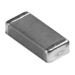
CC0201JRNPO9BN101
Yageo
From $0.05 • 1 mil+ units available from multiple sources
CC0201JRNPO9BN101
Yageo
0201 100 pF 50 V ?5% Tolerance C0G/NP0 Multilayer Ceramic Chip Capacitor
| Distributor | SKU | Stock | MOQ | 1 | 10 | 50 | 100 | 1,000 | 10,000 | |
|---|---|---|---|---|---|---|---|---|---|---|
| DigiKey | 311-2080-1-ND | 332,907 | 1 | $0.10 | $0.02 | $0.01 | $0.01 | $0.00 | $0.00 | Buy |
| Mouser Electronics | 603-CC201JRNPO9BN101 | 72,325 | 1 | $0.10 | $0.02 | $0.02 | $0.01 | $0.01 | $0.00 | |
| Future Electronics | CC0201JRNPO9BN101 | 15,000 | 15,000 | Buy | ||||||
| AVNET Express | CC0201JRNPO9BN101 | 15,000 | 15,000 | Buy | ||||||
| element14 APAC | CC0201JRNPO9BN101 | 15,000 | 500 | $0.01 | $0.01 | Buy | ||||
| TME | CC0201JRNPO9BN101 | 14,900 | Buy | |||||||
| Rutronik | CC0201JRNPO9BN101 | 0 | 300,000 | Buy | ||||||
| Newark | CC0201JRNPO9BN101 | 30,000 | 1 | $0.10 | $0.10 | $0.01 | $0.01 | $0.01 | $0.01 | Buy |
| Farnell | CC0201JRNPO9BN101 | 15,000 | 500 | $0.00 | $0.00 | Buy | ||||
| AVNET Europe | CC0201JRNPO9BN101 | 135,000 | 15,000 | Buy | ||||||
| AVNET Asia Pacific | CC0201JRNPO9BN101 | 0 | 15,000 | Buy | ||||||
| Arrow Europe | CC0201JRNPO9BN101 | 3,525,000 | 15,000 | |||||||
| Arrow North American Components | CC0201JRNPO9BN101 | 495,000 | 15,000 | $0.05 | $0.01 | $0.01 | $0.01 | $0.00 | $0.00 | |
| Verical Marketplace | CC0201JRNPO9BN101 | 3,525,000 | 15,000 | |||||||
| Ameya360 | CC0201JRNPO9BN101 | 210,000 | Buy | |||||||
| Jak Electronics | CC0201JRNPO9BN101 | 1,000,000 | $0.00 | $0.00 | $0.00 | $0.01 | $0.01 | $0.01 | Buy | |
| Utmel | CC0201JRNPO9BN101 | 374,071 | $0.00 | $0.00 | $0.00 | $0.00 | $0.00 | $0.00 | Buy | |
| Win Source | CC0201JRNPO9BN101 | 7,200 | 1 | Buy | ||||||
| Quarktwin Electronic Components | CC0201JRNPO9BN101 | 13,245 | 10 | $0.09 | $0.08 | $0.08 | $0.07 | $0.06 | $0.05 | Buy |
Automotive Safety and ADAS Applications Reference Design

Texas Instruments
Automotive Safety and ADAS Applications Reference Design
Texas Instruments
This reference design utilizes the TPS65310A-Q1 device which is a power management unit ideally suited for camera or radar based vision system to support features like lane departure warning: collision avoidance systems: blindspot detection or night vision. Alongside ADAS end-equipment applications: this PMIC is also suitable for safety applications.
CC2541EM Reference Design
Texas Instruments
CC2541EM Reference Design
Texas Instruments
The CC2541EM (evaluation module) reference design contains schematics and layout files for the CC2541EM module. The reference design demonstrates good techniques for CC2541 decoupling and RF layout. For optimum RF performance: the reference design should be copied accurately.There are several reference designs to choose from; a 4-layer PCB reference design with an SMA antenna connector for RF output matched to 50 ohm or a 2-layer PCB reference design with the option of using an SMA antenna connector for RF output matched to 50 ohm or an on board inverted F antenna.
Single-Ended Input to Differential Output Conversion Circuit Reference Design

Texas Instruments
Single-Ended Input to Differential Output Conversion Circuit Reference Design
Texas Instruments
This TI Precision Verified Design provides the theory: component selection: simulation: PCB design: and measurement details for a single ended input to differential output circuit which converts a single ended input of +0.1V to +2.4V into a differential output of ± 2.3V on a single +2.7V supply. The output range is intentionally limited to maximize linearity. The circuit is composed of 2 amplifiers. One amplifier acts as a buffer and creates a voltage: Vout+. The second amplifier inverts the input and adds a reference voltage to generate Vout-. Both Vout+ and Vout- range from 0.1V to 2.4V. The difference: Vdiff: is the difference between Vout+ and Vout-. This makes the differential output voltage range +2.3V.