
Search results
300VDC-800VDC Input: 54W 4 Channel Outputs: PSR Flyback with SiC-FET Reference Design

Texas Instruments
300VDC-800VDC Input: 54W 4 Channel Outputs: PSR Flyback with SiC-FET Reference Design
Texas Instruments
This design uses low cost primary side regulation (PSR) IC UCC28700 with a SiC-FET for 300VDC-800VDC input range. Four outputs with separated grounds: 25V/19W: 25V/17W: 25V/10.1W: and 25V/8W are generated.
LTC4012CUF Demo Board | Multi-Chemistry 8A Buck Battery Charger with PowerPath Control

Analog Devices Inc.
LTC4012CUF Demo Board | Multi-Chemistry 8A Buck Battery Charger with PowerPath Control
Analog Devices Inc.
Demonstration circuit 1614 features the LTC4012CUF, a multi-chemistry single battery charger controller with PowerPath™ control. The input supply voltage is 13.5V to 20V and is initially configured for a current limit of 10A. The charger float voltage is programmed by jumpers to support 1- to 4- series cells of both Li-Ion/Polymer and Li-iron phosphate (LiFePO4) at 4.2V/cell and 3.6V/cell, for a total of eight settings. The demo board is initially configured for constant-voltage charging of a 12.6V Li-Ion/ Polymer battery and constant-current charging at 8A, though current derating may be necessary due to certain operating conditions.
NCV7342
onsemi
From $0.37 • 1 k+ units available from DigiKey
NCV7342
onsemi
CAN Transceiver, High Speed, Low Power with Standby and VSPLIT pin
| Distributor | SKU | Stock | MOQ | 1 | 10 | 50 | 100 | 1,000 | 10,000 | |
|---|---|---|---|---|---|---|---|---|---|---|
| DigiKey | NCV7342MW3R2GOSCT-ND | 2,608 | 1 | $0.84 | $0.60 | $0.54 | $0.48 | $0.41 | $0.37 | |
| Mouser Electronics | N/A | 0 | 1 |
ADL5375-05EP-EVALZ

Analog Devices Inc.
ADL5375-05EP-EVALZ
Analog Devices Inc.
The ADL5375 is a broadband quadrature modulator designed for operation from 400 MHz to 6 GHz. Its excellent phase accuracy and amplitude balance enable high performance intermediate frequency or direct radio frequency modulation for communication systems.The ADL5375 features a broad baseband bandwidth, along with an output gain flatness that varies no more than 1 dB from 450 MHz to 3.8 GHz. These features, coupled with a broadband output return loss of 14 dB, make the ADL5375 ideally suited for broadband zero IF or low IF-to-RF applications, broadband digital predistortion transmitters, and multiband radio designs.The ADL5375 accepts two differential baseband inputs and a single-ended LO. It generates a single-ended 50 ? output. The two versions offer input baseband bias levels of 500 mV (ADL5375-05) and 1500 mV (ADL5375-15).The ADL5375 is fabricated using an advanced silicon-germanium bipolar process. It is available in a 24-lead, exposed paddle, Pb-free, LFCSP_VQ package. Performance is specified over a ?40?C to +85?C temperature range. A Pb-free evaluation board is also available.Applications Cellular communication systems GSM/EDGE, CDMA2000, W-CDMA, TD-SCDMA WiMAX/broadband wireless access systems Satellite modems
Qi (WPC) Compliant Wireless Charger for Low Power Wearable Applications

Texas Instruments
Qi (WPC) Compliant Wireless Charger for Low Power Wearable Applications
Texas Instruments
TI design TIDA-00318 is suitable for low power wearable device including a Qi compliant wireless receiver (bq51003)and ultra low current 1 cell Li-ion linear charger (bq25100). It features an ultra small size (5x15mm2), capable of low charging currents down to 10mA and up to 250mAwith support of termination currents as low as 1mA. Current design is designed for 135mA charge current application.
Flatlink Data Transmission System Design Overview (Rev. A)

Texas Instruments
Flatlink Data Transmission System Design Overview (Rev. A)
Texas Instruments
FlatLink is a data transmission system that can provide better than a 2:1 reduction in the number of signal lines used for synchronous parallel data bus structures with no loss in data throughput. To do this FlatLink takes single-ended data at clock rates of up to 68 MHz and increases the data signaling rate seven times up to 476 Mbps. The following report provides some design guidelinesfo
Active Clamp Forward, Flyback for Base Station 3.3V@20A and 15V@1.5A
Texas Instruments
Active Clamp Forward, Flyback for Base Station 3.3V@20A and 15V@1.5A
Texas Instruments
PMP2844 uses two UCC2897s to generate two isolated outputs from 36V – 72V. The 3.3V at 20A converter uses an active clamp forward topology with synchronous rectifiers. The 15V at 1.5A converter uses a flyback topology. Both converters are operating at 200KHz to keep the efficiency high.
Using The 5410 Multi-Channel Buffered Serial Port (McBSP) Sub-Address Scheme
Texas Instruments
Using The 5410 Multi-Channel Buffered Serial Port (McBSP) Sub-Address Scheme
Texas Instruments
Due to memory constraints on data page 0 Multi-Channel Buffered Serial Port (McBSP) registers are accessed using a sub-address scheme. This document discusses how data is accessed through the sub-address registers. A code listing is included.
A Low-Cost 12-bit Speech CODEC Using the MSP430F13x
Texas Instruments
A Low-Cost 12-bit Speech CODEC Using the MSP430F13x
Texas Instruments
This application report illustrates a design of a single chip speech codec (ADC and DAC) using the MSP430F133 MCU from Texas Instruments. The ADC part of this codec uses the on chip 12-bit ADC. The DA
12-mm Tape-and-Reel Component-Delivery System
Texas Instruments
12-mm Tape-and-Reel Component-Delivery System
Texas Instruments
The design advances of component pick-and-place automated equipment for board assembly increasingly are pushing the margins of the tape-and-reel packing configurations. The continuing drive for faster assembly reduces the index time and tends to amplify the forces acting on the tape-and-reel component-delivery system. The magnified forces when combined with a high carrier-tape width-to-component
Simple Output Filter Eliminates ISO Amp Output Ripple And Keeps Full Bandwidth
Texas Instruments
Simple Output Filter Eliminates ISO Amp Output Ripple And Keeps Full Bandwidth
Texas Instruments
The ISO120/121/122 isolation amplifiers (ISO amps) have a small (10-20mVp-p typ) residual demodulator ripple at the output. A simple filter can be added to eliminate the output ripple without decreasing the 50kHz signal bandwidth of the ISO amp.
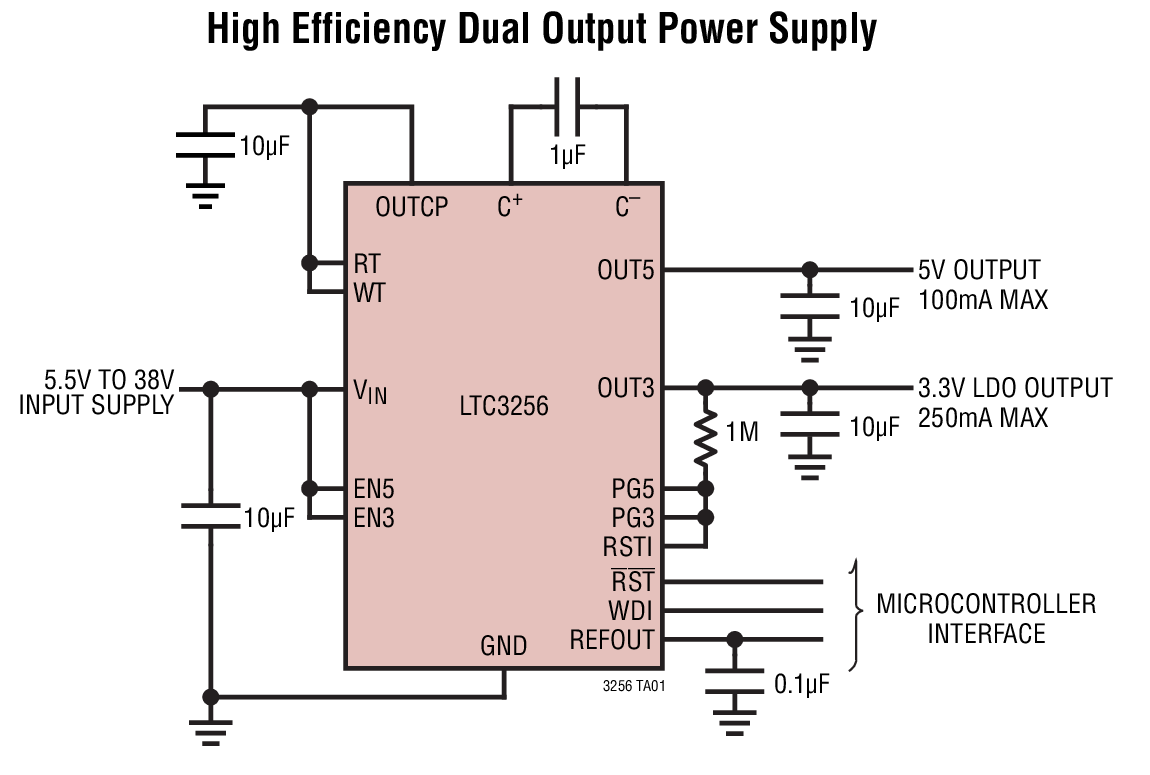
LTC3256 Demo Board | Dual Output Step-Down Charge Pump Plus LDO, 5.5V ≤ VIN ≤ 38V, VOUT1 = 5V @ 100mA, VOUT2 = 3.3V @ 250mA
Analog Devices Inc.
LTC3256 Demo Board | Dual Output Step-Down Charge Pump Plus LDO, 5.5V ≤ VIN ≤ 38V, VOUT1 = 5V @ 100mA, VOUT2 = 3.3V @ 250mA
Analog Devices Inc.
Demonstration Circuit 2375A is a dual output 350mA step down charge pump with a post-regulator LDO and watchdog timer featuring the LTC3256EMSE. The LTC3256 operates with a wide input voltage range from 5.5V to 38V and is engineered for diagnostic coverage in ISO262262 systems. The LTC3256 can provide up to 350mA of output current from a 12V battery with 2W less power dissipation than 2 ideal linear regulators. The DC2375A was populated with automotive grade components for evaluation. Because of the wide input operating range it is possible to exceed the specified operating junction temperature and even reach thermal shutdown with heavy loads. Please refer to the data sheet for additional information on the thermal limitations of the device.
DC1928A

Analog Devices Inc.
DC1928A
Analog Devices Inc.
The LTC3867 is a current mode synchronous step-down switching regulator controller that drives all N-channel power MOSFET stages. Output voltage transient excursions are minimized by use of a nonlinear control architecture to eliminate clock latency issues.The maximum current sense voltage is programmable from 30mV to 75mV, allowing the use of either a discrete sense resistor or the inductor DCR as the sensing element. Programmable DCR temperature compensation allows constant current limit regardless of inductor temperature. Programmable inductor temperature-based thermal shutdown protects the power components from thermal stress. Soft recovery from output shorts or overcurrent minimizes output overshoot.The LTC3867 features a precision 0.6V reference and can regulate output voltages up to 14V from a wide 4V to 38V input supply range. The LTC3867 includes a high speed differential remote sense amplifier. Burst Mode? operation, continuous and pulse-skipping modes are supported. The LTC3867 is available in a 24-lead (4mm ? 4mm) QFN package.Applications Automotive Systems Telecom Systems Industrial Equipment Distributed DC Power Systems
AD9517-3A/PCBZ

Analog Devices Inc.
AD9517-3A/PCBZ
Analog Devices Inc.
The AD9517-31 provides a multi-output clock distribution function with subpicosecond jitter performance, along with an on-chip PLL and VCO. The on-chip VCO tunes from 1.75 GHz to 2.25 GHz. Optionally, an external VCO/VCXO of up to 2.4 GHz can be used.The AD9517-3 emphasizes low jitter and phase noise to maximize data converter performance, and it can benefit other applications with demanding phase noise and jitter requirements.The AD9517-3 features four LVPECL outputs (in two pairs) and four LVDS outputs (in two pairs). Each LVDS output can be reconfigured as two CMOS outputs. The LVPECL outputs operate to 1.6 GHz, the LVDS outputs operate to 800 MHz, and the CMOS outputs operate to 250 MHz.For applications that require additional outputs, a crystal reference input, zero-delay, or EEPROM for automatic configuration at startup, the AD9520 and AD9522 are available. In addition, the AD9516 and AD9518 are similar to the AD9517 but have a different combination of outputs.Each pair of outputs has dividers that allow both the divide ratio and coarse delay (or phase) to be set. The range of division for the LVPECL outputs is 1 to 32. The LVDS/CMOS outputs allow a range of divisions up to a maximum of 1024.The AD9517-3 is available in a 48-lead LFCSP and can be operated from a single 3.3 V supply. An external VCO, which requires an extended voltage range, can be accommodated by connecting the charge pump supply (VCP) to 5 V. A separate LVPECL power supply can be from 2.5 V to 3.3 V (nominal).The AD9517-3 is specified for operation over the industrial range of ?40?C to +85?C.APPLICATIONS Low jitter, low phase noise clock distribution 10/40/100 Gb/sec networking line cards, including SONET, Synchronous Ethernet, OTU2/3/4 Forward error correction (G.710) Clocking high speed ADCs, DACs, DDSs, DDCs, DUCs, MxFEs High performance wireless transceivers ATE and high performance instrumentation 1 AD9517 is used throughout to refer to all the members of the AD9517 family. However, when AD9517-3 is used, it is referring to that specific member of the AD9517 family.
EV-ADF4360-4EB1Z

Analog Devices Inc.
EV-ADF4360-4EB1Z
Analog Devices Inc.
The ADF4360-4 is a fully integrated integer-N synthesizerand voltage-controlled oscillator (VCO). The ADF4360-4 isdesigned for a center frequency of 1600 MHz. In addition, adivide-by-2 option is available, whereby the user gets an RFoutput of between 725 MHz and 875 MHz.Control of all the on-chip registers is through a simple 3-wireinterface. The device operates with a power supply rangingfrom 3.0 V to 3.6 V and can be powered down when not in use.Applications Wireless handsets (DECT, GSM, PCS, DCS, WCDMA) Test equipment Wireless LANs CATV equipment
90VAC-265VAC Input: 12V @ 18W Flyback With Primary-Side Regulation

Texas Instruments
90VAC-265VAC Input: 12V @ 18W Flyback With Primary-Side Regulation
Texas Instruments
The PMP6740 reference design provides 12V at 18W from a universal AC input of 90VAC-265VAC input. This design uses the TL2844 controller with primary side regulation (no optocoupler) for a low cost power solution.