
Search results
WVGA Digital Video SerDes for Automotive TFT LCD Displays w/ OpenLDI Interface Reference Design

Texas Instruments
WVGA Digital Video SerDes for Automotive TFT LCD Displays w/ OpenLDI Interface Reference Design
Texas Instruments
The TIDA-00136 reference design is a high speed serial video interface to connect a remote automotive WVGA TFT LCD display with OpenLDI (LVDS) Interface to a video processing system. It uses TIs FPD-Link II SerDes technology to transmit uncompressed video data over shielded twisted pair or Coax cable. Application examples are rear seat entertainment systems: automotive clusters: and Head Unit Display. This design incorporates the DS99R421Q1-EVK and DS90UR124-Q1 boards together to create the solution.
AD9517-3A/PCBZ

Analog Devices Inc.
AD9517-3A/PCBZ
Analog Devices Inc.
The AD9517-31 provides a multi-output clock distribution function with subpicosecond jitter performance, along with an on-chip PLL and VCO. The on-chip VCO tunes from 1.75 GHz to 2.25 GHz. Optionally, an external VCO/VCXO of up to 2.4 GHz can be used.The AD9517-3 emphasizes low jitter and phase noise to maximize data converter performance, and it can benefit other applications with demanding phase noise and jitter requirements.The AD9517-3 features four LVPECL outputs (in two pairs) and four LVDS outputs (in two pairs). Each LVDS output can be reconfigured as two CMOS outputs. The LVPECL outputs operate to 1.6 GHz, the LVDS outputs operate to 800 MHz, and the CMOS outputs operate to 250 MHz.For applications that require additional outputs, a crystal reference input, zero-delay, or EEPROM for automatic configuration at startup, the AD9520 and AD9522 are available. In addition, the AD9516 and AD9518 are similar to the AD9517 but have a different combination of outputs.Each pair of outputs has dividers that allow both the divide ratio and coarse delay (or phase) to be set. The range of division for the LVPECL outputs is 1 to 32. The LVDS/CMOS outputs allow a range of divisions up to a maximum of 1024.The AD9517-3 is available in a 48-lead LFCSP and can be operated from a single 3.3 V supply. An external VCO, which requires an extended voltage range, can be accommodated by connecting the charge pump supply (VCP) to 5 V. A separate LVPECL power supply can be from 2.5 V to 3.3 V (nominal).The AD9517-3 is specified for operation over the industrial range of ?40?C to +85?C.APPLICATIONS Low jitter, low phase noise clock distribution 10/40/100 Gb/sec networking line cards, including SONET, Synchronous Ethernet, OTU2/3/4 Forward error correction (G.710) Clocking high speed ADCs, DACs, DDSs, DDCs, DUCs, MxFEs High performance wireless transceivers ATE and high performance instrumentation 1 AD9517 is used throughout to refer to all the members of the AD9517 family. However, when AD9517-3 is used, it is referring to that specific member of the AD9517 family.
Automotive 200-VA High Frequency Inverter Design
Texas Instruments
Automotive 200-VA High Frequency Inverter Design
Texas Instruments
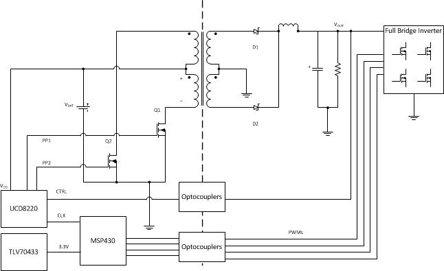
This design presents a low-cost: small size: robust 200-VA DC to AC inverter based on TI’s MSP430 and UCD8220-digitally managed push-pull controller. It is targetted towards car inverters and small-segment inverters for commercial applications. In this design: UCD8220 is used for a boost stage to get 250-V DC from a 12-V battery. The MSP430 acts as a host controller and provides a 100-kHz clock to UCD8220 and drives for output DC-AC bridge. This inverter has a peak efficiency of 90% and has natural cooling and does not require a fan for cooling.

DC1856B-B

Analog Devices Inc.
DC1856B-B
Analog Devices Inc.
The LTM4649 is a complete 10A high efficiency switching mode step-down DC/DC ?Module? regulator in a 9mm ? 15mm ? 4.92 BGA package. Included in the package are the switching controller, power FETs, inductor, and all support components. Operating over an input voltage range of 4.5V to 16V, the LTM4649 supports an output voltage range of 0.6V to 3.3V, set by a single external resistor. This high efficiency design delivers 10A continuous current. Only bulk input and output capacitors are needed.High switching frequency and a current mode architecture enable a very fast transient response to line and load changes without sacrificing stability. The device supports frequency synchronization, programmable multiphase operation, and output voltage tracking for supply rail sequencing.Fault protection features include output overvoltage and overcurrent protection. The LTM4649 is offered in a small 9mm ? 15mm ? 4.92mm BGA package available with SnPb or RoHS compliant terminal finish.Applications Telecom, Networking and Industrial Equipment Point of Load Regulation
LMZ12010 20VIN 10AOUT Simple Switcher? Module Reference Design

Texas Instruments
LMZ12010 20VIN 10AOUT Simple Switcher? Module Reference Design
Texas Instruments
The LMZ13610/8 and LMZ12010/8 SIMPLE SWITCHER® power modules are easy-to-use DC-DC solution capable of driving up to a 10A load. They are available in an innovative package that enhances thermal performance and allows for hand or machine soldering. The LMZ13610/8 can accept an input voltage rail between 6V and 36V and the LMZ12010/8 can accept an input voltage rail between 6V and 20V. The devices can deliver an adjustable and highly accurate output voltage as low as 0.8V and as high as 6V. The control structure is constant frequency PWM. The control loop operates well with low ESR output capacitors such as ceramics. The precision enable input allows for programmable UVLO of the input supply. The external soft-start capacitor facilitates a controlled and adjustable startup rise time of the output. The LMZ13610 and LMZ12010 family is a reliable and robust solution with the following features: loss-less cycle-by-cycle valley current limit to protect for over current or short-circuit fault, thermal shutdown, input under-voltage lockout, and will start up into a pre-biased output. Free-running switching frequency is 350 kHz.
Automotive Power Supply

Texas Instruments
Automotive Power Supply
Texas Instruments
PMP7031 is an automotive dual buck supply with a boost on the input: which enables working down to 3V. It has a low quiesecent current during shutdown and supports various functions needed in an automotive application.
10 µA to 100 mA: 0.05% error: high-side current sensing reference design

Texas Instruments
10 µA to 100 mA: 0.05% error: high-side current sensing reference design
Texas Instruments
This TI Precision Verified Design provides the theory: component selection: simulation: complete PCB schematic and layout: bill of materials: and measured performance of a split-supply: high-side four decade current sensing solution that can accurately detect load currents from 10uA-100mA. The corresponding linear output is from 10mV to 4.9V which enables measurement by common 5V ADCs. The design utilizes the PGA281: an instrumentation amplifier with pin-programmable gain and a wide common-mode voltage range: to provide a more accurate and versatile solution than traditional op amps.See more TI Precision Designs
EVAL-AD4003FMCZ

Analog Devices Inc.
EVAL-AD4003FMCZ
Analog Devices Inc.
The AD4003/AD4007/AD4011 are high accuracy, high speed, low power, 18-bit, Easy Drive, precision successive approximation register (SAR) analog-to-digital converters (ADCs) that operate from a single power supply, VDD. The reference voltage, VREF, is applied externally and can be set independent of the supply voltage. The AD4003/AD4007/AD4011 power scales linearly with throughput. Easy Drive features reduce both signal chain complexity and power consumption while enabling higher channel density. The reduced input current, particularly in high-Z mode, coupled with a long signal acquisition phase, eliminates the need for a dedicated ADC driver. Easy Drive broadens the range of companion circuitry that is capable of driving these ADCs (see Figure 2 in the data sheet).Input span compression eliminates the need to provide a negative supply to the ADC driver amplifier while preserving access to the full ADC code range. The input overvoltage clamp protects the ADC inputs against overvoltage events, minimizing disturbances on the reference pin and eliminating the need for external protection diodes. Fast device throughput up to 2 MSPS allows users to accurately capture high frequency signals and to implement oversampling techniques to alleviate the challenges associated with antialias filter designs. Decreased serial peripheral interface (SPI) clock rate requirements reduce digital input and output power consumption, broadens digital host options, and simplifies the task of sending data across digital isolation. The SPI-compatible serial user interface is compatible with 1.8 V, 2.5 V, 3 V, and 5 V logic by using the separate VIO logic supply.APPLICATIONS Automated test equipment Machine automation Medical equipment Battery-powered equipment Precision data acquisition systems Instrumentation and control systems
85VAC-265VAC Input: 12V/15W Output Green-Mode Flyback

Texas Instruments
85VAC-265VAC Input: 12V/15W Output Green-Mode Flyback
Texas Instruments
The PMP6833 reference design uses the UCC28600 green-mode controller to generate a 12V/15W regulated output. The quasi-resonant switching of the UCC28600 allows this low-cost design to achieve a maximum load efficiency is over 83%: while the no load losses are less than 200mW.
CC2541EM Reference Design
Texas Instruments
CC2541EM Reference Design
Texas Instruments
The CC2541EM (evaluation module) reference design contains schematics and layout files for the CC2541EM module. The reference design demonstrates good techniques for CC2541 decoupling and RF layout. For optimum RF performance: the reference design should be copied accurately.There are several reference designs to choose from; a 4-layer PCB reference design with an SMA antenna connector for RF output matched to 50 ohm or a 2-layer PCB reference design with the option of using an SMA antenna connector for RF output matched to 50 ohm or an on board inverted F antenna.
EVAL-AD7175-2SDZ

Analog Devices Inc.
EVAL-AD7175-2SDZ
Analog Devices Inc.
The AD7175-2 is a low noise, fast settling, multiplexed, 2-/4-channel (fully/pseudo differential) ?-? analog-to-digital converter(ADC) for low bandwidth inputs. It has a maximum channelscan rate of 50 kSPS (20 ?s) for fully settled data. The outputdata rates range from 5 SPS to 250 kSPS.The AD7175-2 integrates key analog and digital signal conditioningblocks to allow users to configure an individual setup foreach analog input channel in use. Each feature can be user selectedon a per channel basis. Integrated true rail-to-rail buffers on theanalog inputs and external reference inputs provide easy to drivehigh impedance inputs. The precision 2.5 V low drift (2 ppm/?C)band gap internal reference (with output reference buffer) addsembedded functionality to reduce external component count.The digital filter allows simultaneous 50 Hz/60 Hz rejection at27.27 SPS output data rate. The user can switch betweendifferent filter options according to the demands of eachchannel in the application. The ADC automatically switchesthrough each selected channel. Further digital processingfunctions include offset and gain calibration registers,configurable on a per channel basis.The device operates with a 5 V AVDD1, or ?2.5 V AVDD1/AVSS,and 2 V to 5 V AVDD2 and IOVDD supplies. The specifiedoperating temperature range is ?40?C to +105?C. The AD7175-2 isin a 24-lead TSSOP package.Applications Process control: PLC/DCS modules Temperature and pressure measurement Medical and scientific multichannel instrumentation Chromatography
ADP121CB-1.5-EVALZ

Analog Devices Inc.
ADP121CB-1.5-EVALZ
Analog Devices Inc.
The ADP121 is a quiescent current, low dropout, linear regulator that operates from 2.3 V to 5.5 V and provides up to 150 mA of output current. The low 135 mV dropout voltage at 150 mA load improves efficiency and allows operation over a wide input voltage range. The low 30 ?A of quiescent current at full load makes the ADP121 ideal for battery-operated portable equipment.The ADP121 is available in output voltages ranging from 1.2 V to 3.3 V. The parts are optimized for stable operation with small 1 ?F ceramic output capacitors. The ADP121 delivers good transient performance with minimal board area.Short-circuit protection and thermal overload protection circuits prevent damage in adverse conditions. The ADP121 is available in a tiny 5-lead TSOT and 4-ball 0.4 mm pitch WLCSP pack-ages and utilizes the smallest footprint solution to meet a variety of portable applications.
RC1206FR-079K31L
Yageo
From $0.05 • 100 k+ units available from multiple sources
RC1206FR-079K31L
Yageo
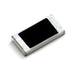
RC Series 1206 0.25 W 9.31 kOhm ?1% ?100 ppm/?C SMT Thick Film Chip Resistor
| Distributor | SKU | Stock | MOQ | 1 | 10 | 50 | 100 | 1,000 | 10,000 | |
|---|---|---|---|---|---|---|---|---|---|---|
| DigiKey | 311-9.31KFRCT-ND | 18,401 | $0.10 | $0.03 | $0.03 | $0.01 | $0.01 | $0.01 | Buy | |
| Mouser Electronics | 603-RC1206FR-079K31L | 8,303 | 1 | $0.10 | $0.03 | $0.03 | $0.02 | $0.01 | $0.01 | Buy |
| Future Electronics | RC1206FR-079K31L | 20,000 | 5,000 | $0.01 | Buy | |||||
| AVNET Express | RC1206FR-079K31L | 0 | 5,000 | $0.00 | Buy | |||||
| element14 APAC | RC1206FR-079K31L | 4,970 | 10 | $0.04 | $0.04 | $0.02 | $0.02 | $0.02 | Buy | |
| TME | RC1206FR-079K31L | 300 | Buy | |||||||
| Rutronik | RC1206FR-079K31L | 35,000 | 5,000 | Buy | ||||||
| Newark | RC1206FR-079K31L | 4,970 | 10 | $0.01 | $0.01 | $0.01 | $0.01 | $0.01 | Buy | |
| Farnell | RC1206FR-079K31L | 4,970 | 500 | $0.01 | $0.01 | Buy | ||||
| AVNET Europe | RC1206FR-079K31L | 0 | 5,000 | $0.00 | Buy | |||||
| Ameya360 | RC1206FR-079K31L | 15,000 | Buy | |||||||
| Jak Electronics | RC1206FR-079K31L | 129,700 | $0.33 | $0.00 | $0.00 | $0.19 | $0.12 | $0.00 | Buy | |
| Utmel | RC1206FR-079K31L | 129,700 | $0.04 | $0.00 | $0.00 | $0.03 | $0.02 | $0.00 | Buy | |
| Quarktwin Electronic Components | RC1206FR-079K31L | 24,779 | 10 | $0.09 | $0.08 | $0.08 | $0.07 | $0.06 | $0.05 | Buy |