
Search results
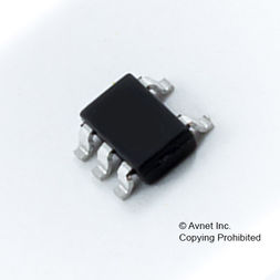
510JCA200M000AAG
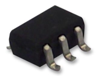
Silicon Laboratories (Silicon Labs)
From $5.07 • 50 units available from AVNET Europe
510JCA200M000AAG
Silicon Laboratories (Silicon Labs)
Crystal Oscillator 200MHz 1.8V 15pF 6-Pin SMD Tray
| Distributor | SKU | Stock | MOQ | 1 | 10 | 50 | 100 | 1,000 | 10,000 | |
|---|---|---|---|---|---|---|---|---|---|---|
| DigiKey | 510JCA200M000AAGR-ND | 0 | 1,000 | $5.09 | $5.09 | $4.25 | $4.25 | |||
| Mouser Electronics | 634-510JCA200M000AAG | 0 | 1 | $5.31 | $5.20 | $5.00 | $4.90 | $4.38 | $4.38 | |
| AVNET Europe | 510JCA200M000AAG | 50 | 1 | $5.21 | $5.17 | $5.10 | $5.07 | $5.07 | $5.07 | Buy |
AD9671EBZ

Analog Devices Inc.
AD9671EBZ
Analog Devices Inc.
The AD9671 is designed for low cost, low power, small size, andease of use for medical ultrasound applications. It contains eightchannels of a VGA with an LNA, a CW harmonic rejection I/Qdemodulator with programmable phase rotation, an AAF, anADC, and a digital demodulator and decimator for dataprocessing and bandwidth reduction.Each channel features a maximum gain of up to 52 dB, a fullydifferential signal path, and an active input preamplifier termination.The channel is optimized for high dynamic performance andlow power in applications where a small package size is critical.The LNA has a single-ended to differential gain that is selectablethrough the serial port interface (SPI). Assuming a 15 MHz noisebandwidth (NBW) and a 21.6 dB LNA gain, the LNA input SNRis 94 dB. In CW Doppler mode, each LNA output drives an I/Qdemodulator that has independently programmable phaserotation with 16 phase settings.Power-down of individual channels is supported to increasebattery life for portable applications. Standby mode allows quickpower-up for power cycling. In CW Doppler operation, theVGA, AAF, and ADC are powered down. The ADC containsseveral features designed to maximize flexibility and minimizesystem cost, such as a programmable clock, data alignment, andprogrammable digital test pattern generation. The digital testpatterns include built-in fixed patterns, built-in pseudorandompatterns, and custom user defined test patterns entered via the SPI.Applications Medical imaging/ultrasound Nondestructive testing (NDT)
CC1101-CC1190EM 869 MHz Reference Design

Texas Instruments
CC1101-CC1190EM 869 MHz Reference Design
Texas Instruments
The CC1101-CC1190EM 869MHz reference design contains schematics and layout files for the CC1101-CC1190EM 869MHz evaluation module. The reference design demonstrates good techniques for CC1101-CC1190 decoupling and RF layout. For optimum RF performance: these parts should be copied accurately. This is a 4-layer reference design with a discrete balun and an SMA antenna connector designed for a single ended 50 ohm antenna. The RF section has been designed and characterized for operation in the 869.4 - 869.65 MHz frequency sub-band (g3): but can also be used for other frequencies in the European 863 - 870 MHz band.
Comparator with Hysteresis Reference Design

Texas Instruments
Comparator with Hysteresis Reference Design
Texas Instruments
This TI Verified Design implements a comparator with hysteresis. Comparators are used to differentiate between two different signal levels. For example: a comparator may differentiate between an over temperature and normal temperature condition. Noise or signal variation at the comparison threshold will cause multiple transitions. Hysteresis sets an upper and lower threshold to eliminate the multiple transitions caused by noise.
Using the Video Port of TMS320DM646x (Rev. A)
Texas Instruments
Using the Video Port of TMS320DM646x (Rev. A)
Texas Instruments
This application report has supplemental information about using the DM646x video port. The tips and tricks in this document are useful in video security applications as well as other applications that make use of the video port.
Implementation of FSK Modulation and Demodulation using CD74HC4046A
Texas Instruments
Implementation of FSK Modulation and Demodulation using CD74HC4046A
Texas Instruments
In telecommunications and signal processing, frequency modulation (FM) is encoding of information on a carrier wave by varying the instantaneous frequency of the wave. Digital data can be encoded and transmitted via carrier wave by shifting the carrier's frequency among a predefined set of frequencies—a technique known as frequency-shift keying (FSK). FSK is widely used in modems, radio-teletype and fax modems, and can also be used to send Morse code.
Frequency-shift keying (FSK) is a frequency modulation scheme in which digital information is transmitted through discrete frequency changes of a carrier wave. This application report discusses logiclevel implementation of binary FSK (BFSK) modulator and demodulator using a phase-locked loop PLL device – CD54HC4046A, CD54HCT4046A, CD74HC4046A, and CD74HCT4046A (hereafter in this document referred to as HC/HCT4046A). BFSK is the simplest FSK, using a pair of discrete frequencies to transmit binary information.
12 Cell 4A Stackable Slave Bidirectional Active Cell Balancer Featuring LTC6804-2 and LTC3300-1(x2)

Analog Devices Inc.
12 Cell 4A Stackable Slave Bidirectional Active Cell Balancer Featuring LTC6804-2 and LTC3300-1(x2)
Analog Devices Inc.
Demonstration Circuit DC2100B-D is a stackable, bidirectional cell balancer slave board using the LTC6804-2 and the LTC3300-1 ICs to achieve active balancing of up to 12 Li-Ion cells. It requires the DC2100B-C for proper operation. The DC2100B-D uses a single LTC6804-2 Multi-Cell Addressable Battery Stack Monitor IC to measure cell voltages and two LTC3300-1 Synchronous Flyback ICs to provide active cell balancing. The DC2100B-C controller board contains a PIC18F47J53 microcontroller, the LTM2884 isolated USB transceiver, the LTC6804-2, two LTC3300-1 ICs, and the LTC6820 isoSPI Interface IC to facilitate isolated communication. Up to seven DC2100B-D boards can be connected to a DC2100B-C to build a stacked system of eight total boards.
AD8556-EVALZ

Analog Devices Inc.
AD8556-EVALZ
Analog Devices Inc.
The AD8556 is a zero-drift, sensor signal amplifier withdigitally programmable gain and output offset. Designed toeasily and accurately convert variable pressure sensor andstrain bridge outputsto a well-defined output voltage range,the AD8556 accurately amplifies many other differential orsingle-ended sensor outputs. The AD8556 uses the ADIpatented low noise auto-zero and DigiTrim? technologies tocreate an incredibly accurate and flexible signal processingsolution in a very compact footprint.Gain is digitally programmable in a wide range from 70 to1,280 through a serial data interface. Gain adjustment canbe fully simulated in-circuit and then permanently programmedwith reliable polyfuse technology. Output offsetvoltage is also digitally programmable and is ratiometric to thesupply voltage. AD8556 also features internal EMI filters on theVNEG, VPOS, FILT and VCLAMP pins.In addition to extremely low input offset voltage, low inputoffset voltage drift, and very high dc and ac CMRR, the AD8556 also includes a pull-up current source at the input pinsand a pull-down current source at the VCLAMP pin. Thisallows open wire and shorted wire fault detection. A low-passfilter function is implemented via a single low cost externalcapacitor. Output clamping set via an external reference voltageallows the AD8556 to drive lower voltage ADCs safely andaccurately.When used in conjunction with an ADC referenced to the samesupply, the system accuracy becomes immune to normal supplyvoltage variations. Output offset voltage can be adjusted with aresolution of better than 0.4% of the difference between VDDand VSS. A lockout trim after gain and offset adjustmentfurther ensures field reliability.The AD8556 is fully specified from ?40?C to +140?C.Operating from single-supply voltages of 2.7 V to 5.5 V, theAD8556 is offered in the 8-lead SOIC_N, and 4 mm ? 4 mm16-lead LFCSP_VQ.ApplicationsAutomotive SensorsPressure and Position SensorsPrecision Current SensingStrain Gages
36-75VDC Input: 32V/3A output with Flyback configuration

Texas Instruments
36-75VDC Input: 32V/3A output with Flyback configuration
Texas Instruments
The PMP4992 reference design provides an isolated 32V at 96W (3A) from a standard 48V telecom bus with 91% efficiency. This design uses the TPS40210 to control a diode rectified flyback converter for a low cost and efficient design.
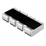
CAY16-5601F4LF
Bourns, Inc.
From $0.05 • 40 units available from multiple sources
CAY16-5601F4LF
Bourns, Inc.
Res Thick Film Array 5.6K Ohm 1% ISOL Molded 8-Pin 1206 Convex SMD Paper T/R
| Distributor | SKU | Stock | MOQ | 1 | 10 | 50 | 100 | 1,000 | 10,000 | |
|---|---|---|---|---|---|---|---|---|---|---|
| DigiKey | CAY16-5601F4LF-ND | 0 | $0.05 | Buy | ||||||
| Mouser Electronics | 652-CAY16-5601F4LF | 0 | 1 | $0.17 | $0.15 | $0.15 | $0.13 | $0.11 | $0.07 | |
| AVNET Express | CAY16-5601F4LF | 10 | 5,000 | $0.01 | Buy | |||||
| element14 APAC | CAY16-5601F4LF | 10 | 10 | $0.12 | $0.12 | $0.07 | $0.07 | $0.07 | Buy | |
| Newark | CAY16-5601F4LF | 10 | 5,000 | $0.02 | Buy | |||||
| Farnell | CAY16-5601F4LF | 10 | 5,000 | $0.05 | Buy | |||||
| AVNET Europe | CAY16-5601F4LF | 0 | 5,000 | $0.03 | Buy |
DC1948A
Analog Devices Inc.
DC1948A
Analog Devices Inc.
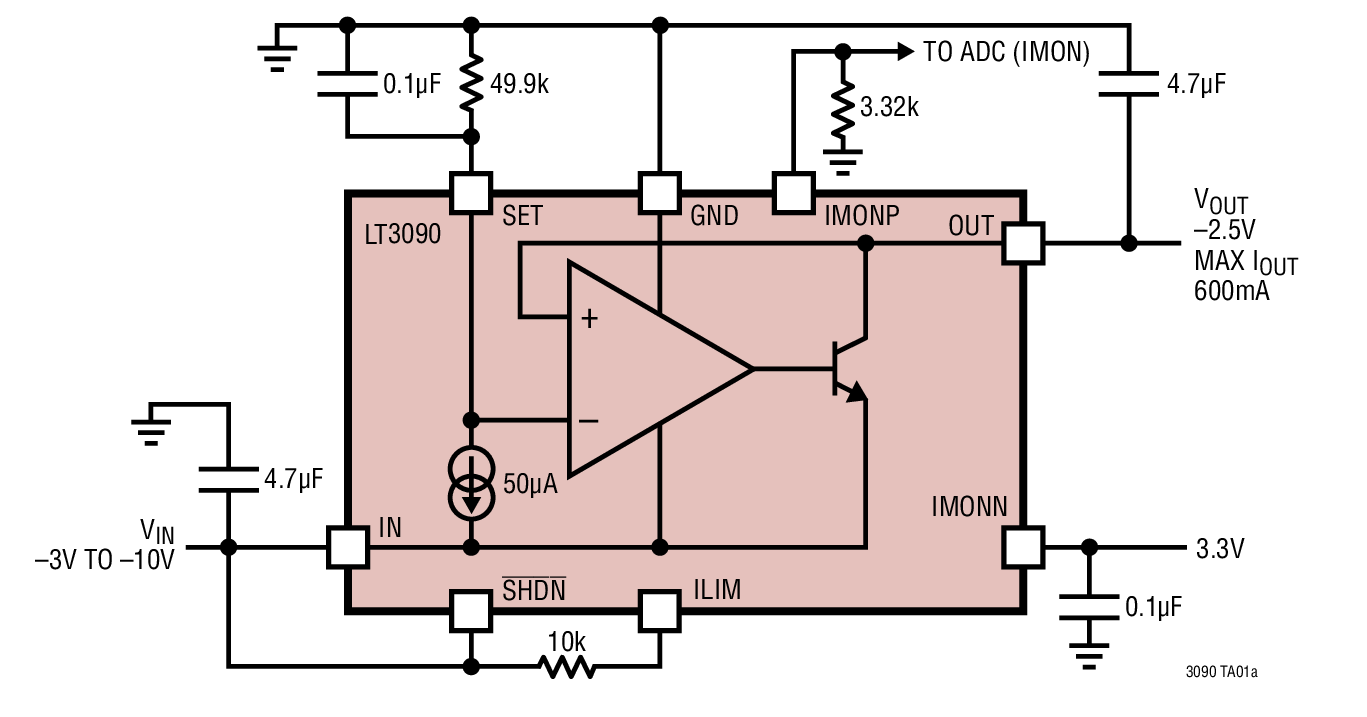
The LT3090 is a 600mA, low dropout negative linear regulator that is easily parallelable to increase output current or spread heat on surface mounted boards. Designed with a precision current reference followed by a high performance rail-to-rail voltage buffer, this regulator finds use in applications requiring precision output, high current with no heat sink, output adjustability to zero and low dropout voltage. The device can also be configured as a 3-terminal floating regulator.The LT3090 features fast transient response, high PSRR and output noise as low as 18?VRMS. The LT3090 generates a wide output voltage range (0V to ?32V) while maintaining unity gain operation. This yields virtually constant bandwidth, load regulation, PSRR and noise, regardless of the programmed output voltage.The LT3090 supplies 600mA at a typical dropout voltage of 300mV. Operating quiescent current is nominally 1mA and drops to << 1?A in shutdown. A single resistor adjusts the LT3090?s precision programmable current limit. The LT3090?s positive or negative current monitor either sources a current (0.5mA/A) or sinks a current (1mA/A) proportional to output current. Built-in protection includes reverse output protection, internal current limit with foldback and thermal shutdown with hysteresis.Applications Post Regulator for Switching Supplies Low Noise Instrumentation and RF Supplies Rugged Industrial Supplies Precision Power Supplies
CR0603-FX-20R5ELF

Bourns, Inc.
From $0.00 • 1 k+ units available from Mouser Electronics
CR0603-FX-20R5ELF
Bourns, Inc.
Res Thick Film 0603 20.5 Ohm 1% 1/10W ±100ppm/°C Molded SMD SMD Paper Tape on Plastic Reel
| Distributor | SKU | Stock | MOQ | 1 | 10 | 50 | 100 | 1,000 | 10,000 | |
|---|---|---|---|---|---|---|---|---|---|---|
| DigiKey | CR0603-FX-20R5ELF-ND | 0 | Buy | |||||||
| Mouser Electronics | 652-CR0603FX-20R5ELF | 9,500 | 1 | $0.14 | $0.03 | $0.03 | $0.02 | $0.01 | $0.01 | |
| AVNET Express | CR0603-FX-20R5ELF | 0 | 5,000 | Buy | ||||||
| Newark | CR0603-FX-20R5ELF | 0 | 25,000 | $0.00 | Buy | |||||
| AVNET Europe | CR0603-FX-20R5ELF | 0 | 5,000 | Buy |
ADP1764-ADJ-EVALZ

Analog Devices Inc.
ADP1764-ADJ-EVALZ
Analog Devices Inc.
The ADP1764 is a low noise, low dropout (LDO) linear regulator. It is designed to operate from a single input supply with an input voltage as low as 1.10 V without the requirement of an external bias supply to increase efficiency and provide up to 4 A of output current (IOUT).The low 47 mV typical dropout voltage at a 4 A load allows theADP1764 to operate with a small headroom while maintainingregulation and providing better efficiency.The ADP1764 is optimized for stable operation with small 22 ?F ceramic output capacitors. The ADP1764 delivers optimal transientperformance with minimal printed circuit board (PCB) area.The ADP1764 is available in fixed output voltages ranging from 0.55 V to 1.5 V. The output voltage (VOUT) of the adjustableoutput model can be set from 0.5 V to 1.5 V through an external resistor connected between VADJ and ground.The ADP1764 has an externally programmable soft start time by connecting a capacitor to the SS pin. Short-circuit and thermaloverload protection circuits prevent damage in adverse conditions.The ADP1764 is available in a small, 16-lead LFCSP package forthe smallest footprint solution to meet a variety of applications.Applications Regulation to noise sensitive applications such as radio frequency (RF) transceivers, analog-to-digital converter (ADC) and digital-to-analog converter (DAC) circuits, phase-locked loops (PLLs), voltage controlled oscillators (VCOs) and clocking integrated circuits Field-programmable gate array (FPGA) and digital signal processor (DSP) supplies Medical and healthcare Industrial and instrumentation
Altera Arria V GX FPGA Power Solution Reference Design

Texas Instruments
Altera Arria V GX FPGA Power Solution Reference Design
Texas Instruments
The PMP9449 reference design provides all the power supply rails necessary to power Altera's Arria® V GX family of FPGAs. It utilizes a TPS38600 to monitor the input supply and provide power on sequencing. This design features low cost: small footprint discrete ICs and is powered from a single 5V input.