
Search results
Boost Converter LED Driver Using 9V – 24V Input Range

Texas Instruments
Boost Converter LED Driver Using 9V – 24V Input Range
Texas Instruments
This reference design uses the TPS40211 current mode controller in a boost converter to regulate the current in a series string of 12 LEDs (42V) at 0.35A. Efficiency is greater than 94%.
AN-386 A Non-Complementary Audio Noise Reduction System (Rev. C)

Texas Instruments
AN-386 A Non-Complementary Audio Noise Reduction System (Rev. C)
Texas Instruments
The popularity of companding or complementary noise reduction systems is self-evident. Nearly allmedium to high quality cassette tape decks include either Dolby®B or Dolby C type noise reduction. Ascant few have different systems such as dbx or Hi-Com. The universal appeal of compandors to n.r.system designers is the amount of noise reduction they can offer yet one of the major reasons t
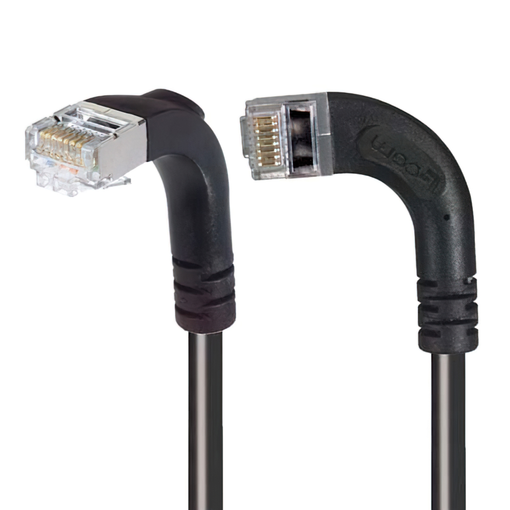
TRD695SRA11BLK-10
L-com
From $6.49 • 4 units available from Newark
TRD695SRA11BLK-10
L-com
Modular Cable Plug to Plug, Right Angle 8p8c (RJ45, Ethernet) 10.00' (3.05m) Shielded
| Distributor | SKU | Stock | MOQ | 1 | 10 | 50 | 100 | 1,000 | 10,000 | |
|---|---|---|---|---|---|---|---|---|---|---|
| DigiKey | 5073-TRD695SRA11BLK-10-ND | 0 | $7.51 | $7.51 | $7.51 | $7.51 | $7.51 | $7.51 | Buy | |
| element14 APAC | TRD695SRA11BLK-10 | 0 | 1 | $30.79 | $26.94 | $22.32 | $20.02 | $18.48 | $18.48 | Buy |
| Newark | TRD695SRA11BLK-10 | 4 | 1 | $6.49 | $6.49 | $6.49 | $6.49 | $6.49 | $6.49 | Buy |
| Farnell | TRD695SRA11BLK-10 | 0 | 1 | $24.17 | $17.52 | $15.71 | $15.71 | $15.71 | $15.71 | Buy |
CC1120EM 955 MHz Reference Design
Texas Instruments
CC1120EM 955 MHz Reference Design
Texas Instruments
The CC1120 955MHz EM reference design contains schematics and layout files for the CC1120EM 955MHz evaluation module. The reference design demonstrates good techniques for CC1120 decoupling and RF layout. For optimum RF performance: these parts should be copied accurately. This is a 4-layer reference design with a discrete balun and an SMA antenna connector designed for a single ended 50 ohm antenna. The RF section has been designed and characterized for operation in the 955 MHz frequency band.
DC1856B-B

Analog Devices Inc.
DC1856B-B
Analog Devices Inc.
The LTM4649 is a complete 10A high efficiency switching mode step-down DC/DC ?Module? regulator in a 9mm ? 15mm ? 4.92 BGA package. Included in the package are the switching controller, power FETs, inductor, and all support components. Operating over an input voltage range of 4.5V to 16V, the LTM4649 supports an output voltage range of 0.6V to 3.3V, set by a single external resistor. This high efficiency design delivers 10A continuous current. Only bulk input and output capacitors are needed.High switching frequency and a current mode architecture enable a very fast transient response to line and load changes without sacrificing stability. The device supports frequency synchronization, programmable multiphase operation, and output voltage tracking for supply rail sequencing.Fault protection features include output overvoltage and overcurrent protection. The LTM4649 is offered in a small 9mm ? 15mm ? 4.92mm BGA package available with SnPb or RoHS compliant terminal finish.Applications Telecom, Networking and Industrial Equipment Point of Load Regulation
EVAL-AD7706EBZ

Analog Devices Inc.
EVAL-AD7706EBZ
Analog Devices Inc.
The AD7705?/ AD7706 are complete analog front ends for low frequency measurement applications. These 2-/3-channel devices can accept low level input signals directly from a transducer and produce serial digital output. The devices employ a ?-? conversion technique to realize up to 16 bits of no missing codes performance. The selected input signal is applied to a proprietary, programmable-gain front end based around an analog modulator. The modulator output is processed by an on-chip digital filter. The first notch of this digital filter can be programmed via an on-chip control register, allowing adjustment of the filter cutoff and output update rate. The AD7705 / AD7706 devices operate from a single 2.7 V to 3.3 V or 4.75 V to 5.25 V supply. The AD7705 features two fully differential analog input channels; the AD7706 features three pseudo differential input channels. Both devices feature a differential reference input. Input signal ranges of 0 mV to 20 mV through 0 V to 2.5 V can be incorporated on both devices when operating with a VDD of 5 V and a reference of 2.5 V. They can also handle bipolar input signal ranges of ?20 mV through ?2.5 V, which are referenced to the AIN(?) inputs on the AD7705 and to the COMMON input on the AD7706.The AD7705 / AD7706 devices, with a 3 V supply and a 1.225 V reference, can handle unipolar input signal ranges of 0 mV to 10 mV through 0 V to 1.225 V. The devices can accept bipolar input ranges of ?10 mV through ?1.225 V. Therefore, the AD7705 / AD7706 devices perform all signal conditioning and conversion for a 2-channel or 3-channel system. The AD7705 / AD7706 are ideal for use in smart, microcontroller, or DSP-based systems. The devices feature a serial interface that can be configured for 3-wire operation. Gain settings, signal polarity, and update rate selection can be configured in software using the input serial port. The parts contains self-calibration and system calibration options to eliminate gain and offset errors on the part itself or in the system. CMOS construction ensures very low power dissipation, and the power-down mode reduces the standby power consumption to 20 ?W typ. These parts are available in a 16-lead, wide body (0.3 inch), plastic dual in-line package (DIP); a 16-lead, wide body (0.3 inch), standard small outline (SOIC) package; and a low profile, 16-lead, thin shrink small outline package (TSSOP).
C1005X6S1E683K050BC
TDK Corporation
From $0.01 • 10 k+ units available from DigiKey
C1005X6S1E683K050BC
TDK Corporation
Cap Ceramic 0.068uF 25V X6S 10% SMD 0402 105°C Punched Paper T/R
| Distributor | SKU | Stock | MOQ | 1 | 10 | 50 | 100 | 1,000 | 10,000 | |
|---|---|---|---|---|---|---|---|---|---|---|
| DigiKey | 445-13905-1-ND | 19,050 | $0.12 | $0.09 | $0.09 | $0.04 | $0.02 | $0.01 | Buy | |
| AVNET Express | C1005X6S1E683K050BC | 0 | 10,000 | Buy | ||||||
| Newark | C1005X6S1E683K050BC | 0 | $0.01 | $0.01 | $0.01 | $0.01 | $0.01 | $0.01 | Buy | |
| Quarktwin Electronic Components | C1005X6S1E683K050BC | 28,991 | 10 | Buy |
EV2HMC788ALP2

Analog Devices Inc.
EV2HMC788ALP2
Analog Devices Inc.
The HMC788A is a 0.01 GHz to 10 GHz, gain block, monolithic microwave integrated circuit (MMIC) amplifier using gallium arsenide (GaAs), pseudomorphic high electron mobility transistor (pHEMT) technology.This 2 mm ? 2 mm LFCSP amplifier can be used as either a cascadable 50 ? gain stage, or to drive the local oscillator (LO) port of many of the single and double balanced mixers from Analog Devices, Inc. with up to 20 dBm output power.The HMC788A offers 14 dB of gain and an output IP3 of 33 dBm while requiring only 76 mA from a 5 V supply.The Darlington feedback pair exhibits reduced sensitivity to normal process variations and yields excellent gain stability over temperature while requiring a minimal number of external bias components.Applications Cellular, 3G, LTE, WiMAX, and 4G LO driver applications Microwave radio Test and measurement equipment Ultra wideband (UWB) communications
SEPIC (5V@250mA) for Auxiliary Bias Supply

Texas Instruments
SEPIC (5V@250mA) for Auxiliary Bias Supply
Texas Instruments
The PMP5298 reference design provides an isolated 5V at 250mA from a 120VAC/60Hz input in less than 1 square inch of board space. This design uses the UCC3813-5 in a non-isolated SEPIC topology. The SEPIC clamping capacitor reduces ringing on the drain of the MOSFET and recaptures leakage energy to improve efficiency.
Hand-to-Hand Body Composition Meter Reference Design with BLE Connectivity

Texas Instruments
Hand-to-Hand Body Composition Meter Reference Design with BLE Connectivity
Texas Instruments
This reference design is for a complete hand-held body composition or fat loss monitor end equipment featuring TI signal chain: power: and connectivity components. With TI's AFE4300 body composition AFE: you can accelerate your body composition design to develop more quickly. This reference design also includes the full BLE connectivity design for easy interface to BLE enabled smartphones: tablets: etc.
MUR2X100A10
GeneSiC
From $25.84 • 10 k+ units available from Quarktwin Electronic Components
MUR2X100A10
GeneSiC
1000V 200A SOT-227 Silicon Rectifier Module - Super Fast Recovery (Standard Configuration)
| Distributor | SKU | Stock | MOQ | 1 | 10 | 50 | 100 | 1,000 | 10,000 | |
|---|---|---|---|---|---|---|---|---|---|---|
| DigiKey | MUR2X100A10-ND | 0 | $22.94 | $22.94 | $22.94 | $22.94 | Buy | |||
| Mouser Electronics | 905-MUR2X100A10 | 0 | 40 | $21.96 | $20.41 | $16.79 | $16.79 | |||
| Newark | MUR2X100A10 | 0 | 156 | $0.00 | $0.00 | $0.00 | $0.00 | $0.00 | $0.00 | Buy |
| Quarktwin Electronic Components | MUR2X100A10 | 39,475 | 10 | $43.76 | $39.39 | $39.39 | $35.45 | $28.71 | $25.84 | Buy |
EVAL-AD7403FMCZ

Analog Devices Inc.
EVAL-AD7403FMCZ
Analog Devices Inc.
The AD7403 is a high performance, second-order, ?-? modulator that converts an analog input signal into a high speed, single-bit data stream, with on-chip digital isolation based on Analog Devices, Inc., iCoupler? technology. The AD7403 operates from a 5 V (VDD1) power supply and accepts a differential input signal of ?250 mV (?320 mV full-scale). The differential input is ideally suited to shunt voltage monitoring in high voltage applications where galvanic isolation is required.The analog input is continuously sampled by a high performance analog modulator, and converted to a ones density digital output stream with a data rate of up to 20 MHz. The original information can be reconstructed with an appropriate digital filter to achieve 88 dB signal to noise ratio (SNR) at ?78.1 kSPS. The serial input/output can use a 5 V or a 3 V supply (VDD2).The serial interface is digitally isolated. High speed complementary metal oxide semiconductor (CMOS) technology, combined with monolithic transformer technology, means the on-chip isolation provides outstanding performance characteristics, superior to alternatives such as optocoupler devices. The AD7403 device is offered in a 16-lead, wide-body SOIC package and has an operating temperature range of ?40?C to +125?C. The AD7403-8 device is offered in an 8-lead, wide-body SOIC package and has an operating temperature range of ?40?C to +105?C.Applications Shunt current monitoring AC motor controls Power and solar inverters Wind turbine inverters Data acquisition systems Analog-to-digital and opto-isolator replacements
TMS320C6000 EMIF to External Flash Memory (Rev. A)
Texas Instruments
TMS320C6000 EMIF to External Flash Memory (Rev. A)
Texas Instruments
Interfacing external flash memory to the Texas Instruments TMS320C6000™ digital signal processor (DSP) is simple compared to previous generations of TI DSPs. The TMS320C6000 advanced external memory interface (EMIF) provides a glueless interface to a variety of external memory devices.
This document describes the following:
- EMIF control registers and asynchronous interface signals<
Reference Design for High-Gain Multistage Amplifier

Texas Instruments
Reference Design for High-Gain Multistage Amplifier
Texas Instruments
Using the LMH6629 and OPA684 op amps: this reference design deals with the difficulties and limitations of developing very high gain: multistage amplifier circuits. Supported by a full scale application report including theory: simulations: board design and evaluation: this design can be easily adjusted for a given application.
ADRF5026-EVALZ-292

Analog Devices Inc.
ADRF5026-EVALZ-292
Analog Devices Inc.
The ADRF5026 is a nonreflective, single-pole, double-throw (SPDT) radio frequency (RF) switch manufactured in a silicon process.The ADRF5026 operates from 100 MHz to 44 GHz with better than 3.8 dB of insertion loss and 45 dB of isolation. The ADRF5026 features an all off control, where both RF ports are in an isolation state. The ADRF5026 has a nonreflective design and both of the RF ports are internally terminated to 50 ?. The ADRF5026 requires a dual-supply voltage of +3.3 V and ?3.3 V. The device employs complimentary metal-oxide semiconductor/low-voltage transistor-transistor logic (CMOS/LVTTL) logic-compatible controls.The ADRF5026 is pin-compatible with the ADRF5027 low frequency cutoff version, which operates from 9 kHz to 44 GHz. The ADRF5026 RF ports are designed to match a characteristic impedance of 50 ?. For ultrawideband products, impedance matching on the RF transmission lines can further optimize high frequency insertion loss and return loss characteristics. Refer to the Narrow-Band Impedance Matching section for an example of a matched circuit that achieves a flat insertion loss response of 2.4 dB from 28 GHz to 43 GHz.The ADRF5026 comes in a 20-terminal, 3 mm ? 3 mm, RoHS-compliant, land grid array (LGA) package and can operate from ?40?C to +105?C.The ADRF5026 supports defense and aerospace applications (AQEC).Applications Industrial scanners Test and instrumentation Cellular infrastructure: 5G mmWave Military radios, radars, electronic counter measures (ECMs) Microwave radios and very small aperture terminals (VSATs)