
Search results
XC3S50AN-5TQG144C

AMD
From $96.44 • 28 units available from multiple sources
XC3S50AN-5TQG144C
AMD
FPGA Spartan-3AN Family 50K Gates 1584 Cells 770MHz 90nm Technology 1.2V 144-Pin TQFP
| Distributor | SKU | Stock | MOQ | 1 | 10 | 50 | 100 | 1,000 | 10,000 | |
|---|---|---|---|---|---|---|---|---|---|---|
| DigiKey | 122-1590-ND | 8 | 1 | $46.28 | $46.28 | $46.28 | $46.28 | $46.28 | $46.28 | Buy |
| Mouser Electronics | 217-C3S50AN-5TQG144C | 0 | 1 | |||||||
| AVNET Express | XC3S50AN-5TQG144C | 0 | 1 | $33.40 | $33.40 | $33.40 | $33.40 | $33.40 | $33.40 | Buy |
| AVNET Europe | XC3S50AN-5TQG144C | 20 | 60 | $96.44 | $96.44 | $96.44 | Buy |
EV-ADA4571RSDZ

Analog Devices Inc.
EV-ADA4571RSDZ
Analog Devices Inc.
The ADA4571 is an anisotropic magnetoresistive (AMR) sensorwith integrated signal conditioning amplifiers and ADC drivers.The ADA4571 produces two analog outputs that indicate theangular position of the surrounding magnetic field.The ADA4571 consists of two die within one package, an AMRsensor, and a fixed gain (G = 40 nominally) instrumentationamplifier. The ADA4571 delivers clean and amplified cosineand sine output signals related to the angle of a rotatingmagnetic field. The output voltage range is ratiometric to thesupply voltage.The sensor contains two Wheatstone bridges, at a relative angleof 45? to one another. A rotating magnetic field in the x-ysensor plane delivers two sinusoidal output signals with thedouble frequency of the angle (?) between sensor and magneticfield direction. Within a homogeneous field in the x-y plane,the output signals are independent of the physical placement inthe z direction (air gap).The ADA4571 is available in an 8-lead SOIC package.Product Highlights Contactless angular measurement. Measures magnetic field direction rather than field intensity. Minimum sensitivity to air gap variations. Large working distance. Excellent accuracy, even for weak saturation fields. Minimal thermal and lifetime drift. Negligible hysteresis. Single chip solution.Applications Absolute position measurement (linear and angle) Brushless dc motor control and positioning Actuator control and positioning Contactless angular measurement and detection Magnetic angular position sensing
6W Boost Converter Optimized for Low Profile/Small Area

Texas Instruments
6W Boost Converter Optimized for Low Profile/Small Area
Texas Instruments
This single cell Li-Ion battery input boost converter provides a 5.3V output at 1.1A (5.8W). It achieves 90% efficiency at full load and operates at 1MHz. PMP7426 uses the TPS55340 high voltage boost converter.
LT3754EUH Demo Board | 16-Channel Boost LED Driver, 20V ≤ VIN ≤ 28V, VLED = 55V @ 50mA

Analog Devices Inc.
LT3754EUH Demo Board | 16-Channel Boost LED Driver, 20V ≤ VIN ≤ 28V, VLED = 55V @ 50mA
Analog Devices Inc.
DC1436A is a 16-Channel High Voltage Boost LED Driver featuring the LT3754. The LT3754 drives up to 50mA per string and has a maximum LED string voltage of 45V. The VIN terminal is powered from an 8V to 14V input supply and is distinct from the 24V PVIN supply (20V to 28V) for best thermal performance. Overvoltage protection is set at 55V in case the LEDs are removed from the circuit. If the LEDs are opened, the FAULT terminal output flag goes low and reports the fault condition. If one or more of the 16 LED channels is not used, its LED pin or terminal should be tied to VOUT (LED+) to disable it. Multiple channels can be tied in parallel by tying their LED1-LED16 pins together.
Improving the Performance of Traditional Flyback-Topology With Two-Switch ?Appro

Texas Instruments
Improving the Performance of Traditional Flyback-Topology With Two-Switch ?Appro
Texas Instruments
This application note explains the basic operation of the two-switch Flyback-power stage, and clarifies benefits and design restrictions not present in traditional Flyback-topology. Power st
LTC3219EUD Demo Board | 9-Channel Charge Pump LED Driver, 2.9V ≤ VIN ≤ 5.5V, VLED = up to 5V @ 28mA per LED (DC590 Requires)

Analog Devices Inc.
LTC3219EUD Demo Board | 9-Channel Charge Pump LED Driver, 2.9V ≤ VIN ≤ 5.5V, VLED = up to 5V @ 28mA per LED (DC590 Requires)
Analog Devices Inc.
Demonstration circuit 1055 is a 250mA Universal Nine Channel Multimode (1x, 1.5x, 2x) Charge Pump LED Driver with two RGB displays and three white LEDs featuring the LTC3219. The LTC3219 is a low noise charge pump designed to drive nine universal LED current sources. The input voltage range is 2.9V to 5.5V. Each channel provides 28mA of LED current. The LTC3219 requires only five small ceramic capacitors to form a complete LED power supply and current controller. The maximum display currents are set with an internal precision current reference. On/Off blinking, gradation, and intensity are achieved via an I2C serial interface. There are 64 dimming states available for the universal LEDs. The DC590 controller board is required for proper operation.
EVAL-AD5677RSDZ
Analog Devices Inc.
EVAL-AD5677RSDZ
Analog Devices Inc.
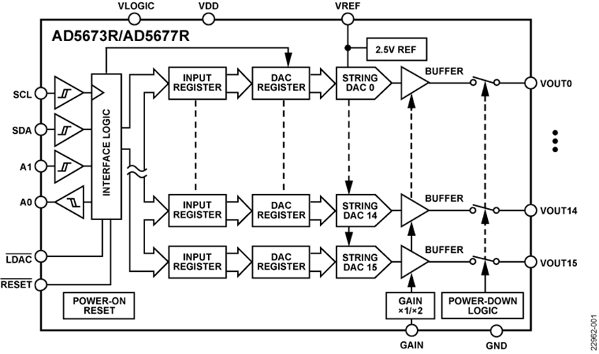
The AD5673R/AD5677R are low power, 16-channel, 12-/16-bit, buffered voltage output, digital-to-analog converters (DACs) that include a 2.5 V, 2 ppm/?C internal reference (enabled by default), and a gain select pin, resulting in a full-scale output of 2.5 V (gain = 1) or 5 V (gain = 2). The devices operate from a single, 2.7 V to 5.5 V supply range and are guaranteed monotonic by design. The AD5673R/AD5677R are available in a 28-lead lead frame chip scale package (LFCSP) and incorporate a power-on reset (POR) circuit that ensures that the DAC outputs power up to and remain at zero scale or midscale until a valid write. The AD5673R/AD5677R contain a power-down mode that reduces the current consumption to 2 ?A typical.Applications Optical transceivers Base station power amplifiers Process control (programmable logic controller (PLC) input/output cards) Industrial automation Data acquisition systems Product Highlights High channel density: 16 channels in 4 mm ? 4 mm LFCSP. High relative accuracy (INL). AD5673R (12-bit): ?1 LSB maximum. AD5677R (16-bit): ?4 LSB maximum. Low drift, 2.5 V, on-chip reference.
TFT LCD Display Power Supply Solutions Using the TPS65100 Triple Output Supply
Texas Instruments
TFT LCD Display Power Supply Solutions Using the TPS65100 Triple Output Supply
Texas Instruments
The reference design and application examples shown in this document highlight the typical applications for the TPS65100 in TFT LCD displays for notebooks and monitors. The TPS65100 offers a compact and small power supply solution that provides all three voltages required by TFT LCD displays. The auxiliary linear regulator controller can be used to generate a 3.3-V logic power rail for systems pow
TSC2046 WinCE 5.0 Driver
Texas Instruments
TSC2046 WinCE 5.0 Driver
Texas Instruments
The TSC2046 Microsoft™ Windows™ CE 5.0 touch driver has been developed and the code has been tested on an Intel™ MainStone II development platform. This application report discusses the TSC2046 driver the Windows CE 5.0 driver's code and structure and the installations. To download software files see SBAC071.
AD9517-3A/PCBZ

Analog Devices Inc.
AD9517-3A/PCBZ
Analog Devices Inc.
The AD9517-31 provides a multi-output clock distribution function with subpicosecond jitter performance, along with an on-chip PLL and VCO. The on-chip VCO tunes from 1.75 GHz to 2.25 GHz. Optionally, an external VCO/VCXO of up to 2.4 GHz can be used.The AD9517-3 emphasizes low jitter and phase noise to maximize data converter performance, and it can benefit other applications with demanding phase noise and jitter requirements.The AD9517-3 features four LVPECL outputs (in two pairs) and four LVDS outputs (in two pairs). Each LVDS output can be reconfigured as two CMOS outputs. The LVPECL outputs operate to 1.6 GHz, the LVDS outputs operate to 800 MHz, and the CMOS outputs operate to 250 MHz.For applications that require additional outputs, a crystal reference input, zero-delay, or EEPROM for automatic configuration at startup, the AD9520 and AD9522 are available. In addition, the AD9516 and AD9518 are similar to the AD9517 but have a different combination of outputs.Each pair of outputs has dividers that allow both the divide ratio and coarse delay (or phase) to be set. The range of division for the LVPECL outputs is 1 to 32. The LVDS/CMOS outputs allow a range of divisions up to a maximum of 1024.The AD9517-3 is available in a 48-lead LFCSP and can be operated from a single 3.3 V supply. An external VCO, which requires an extended voltage range, can be accommodated by connecting the charge pump supply (VCP) to 5 V. A separate LVPECL power supply can be from 2.5 V to 3.3 V (nominal).The AD9517-3 is specified for operation over the industrial range of ?40?C to +85?C.APPLICATIONS Low jitter, low phase noise clock distribution 10/40/100 Gb/sec networking line cards, including SONET, Synchronous Ethernet, OTU2/3/4 Forward error correction (G.710) Clocking high speed ADCs, DACs, DDSs, DDCs, DUCs, MxFEs High performance wireless transceivers ATE and high performance instrumentation 1 AD9517 is used throughout to refer to all the members of the AD9517 family. However, when AD9517-3 is used, it is referring to that specific member of the AD9517 family.
18Vdc-60Vdc Input: 3.3V @ 30A Output: 93% Efficient Active Clamp Forward

Texas Instruments
18Vdc-60Vdc Input: 3.3V @ 30A Output: 93% Efficient Active Clamp Forward
Texas Instruments
The PMP8252 reference design provides 3.3V at 30A from a wide range 18V-60V telecom input with a peak efficiency that is greater than 93%. This design uses the UCC2897A active clamp controller along with Texas Instruments' NexFET power MOSFETs for synchronous rectification.
Reinforced Isolated IGBT Gate Drive Flyback Power Supply with 8 Outputs Reference Design

Texas Instruments
Reinforced Isolated IGBT Gate Drive Flyback Power Supply with 8 Outputs Reference Design
Texas Instruments
This reference design provides reinforced isolated positive and negative voltage rails required for Insulated Gate Bipolar Transistor (IGBT) gate drivers from a single 24-volt DC input supply. Utilizing a flyback isolated control topology: this reference design provides isolation compliant to IEC61800-5: and generates power rails for all three arms of the 3-phase inverter from a single transformer. The output power is currently set at 2W/IGBT but can be scaled up for higher power IGBTs by changing the transformer design.
DC2095A-C
Analog Devices Inc.
DC2095A-C
Analog Devices Inc.
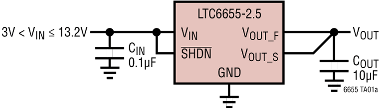
The LTC6655 is a complete family of precision bandgap voltage references, offering exceptional noise and drift performance. This low noise and drift is ideally suited for the high resolution measurements required by instrumentation and test equipment. In addition, the LTC6655 is fully specified over the temperature range of ?40?C to 125?C, ensuring its suitability for demanding automotive and industrial applications. Advanced curvature compensation allows this bandgap reference to achieve a drift of less than 2ppm/?C with a predictable temperature characteristic and an output voltage accurate to ?0.025%, reducing or eliminating the need for calibration.The LTC6655LN Low Noise comes with a noise reduction pin that enables reduction of wideband noise with the addition of a single capacitor.The LTC6655 can be powered from as little as 500mV above the output voltage to as much as 13.2V. Superior load regulation with source and sink capability, coupled with exceptional line rejection, ensures consistent performance over a wide range of operating conditions. A shutdown mode is provided for low power applications.The LTC6655 references are offered in an 8-lead MSOP package and an 8-lead LS8 package. The LS8 is a 5mm ? 5mm surface mount hermetic package that provides outstanding stability.APPLICATIONS Instrumentation and Test Equipment High Resolution Data Acquisition Systems Weigh Scales Precision Battery Monitors Precision Regulators Medical Equipment