
Search results
DC2071A-B
Analog Devices Inc.
DC2071A-B
Analog Devices Inc.
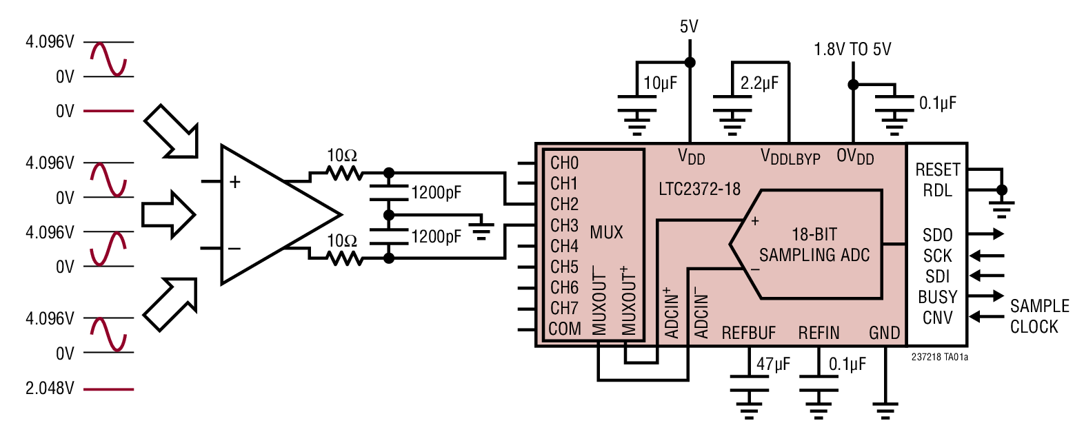
The LTC2372-18 is a low noise, high speed, 8-channel 18-bit successive approximation register (SAR) ADC. Operating from a single 5V supply, the LTC2372-18 has a highly configurable, low crosstalk 8-channel input multiplexer, supporting fully differential, pseudo-differential unipolar and pseudo-differential bipolar analog input ranges. The LTC2372-18 achieves ?2.75LSB INL (maximum) in all input ranges, no missing codes at 18-bits and 100dB (fully differential)/ 95dB (pseudo-differential) SNR (typical).The LTC2372-18 has an onboard low drift (20ppm/?C max) 2.048V temperature-compensated reference and a single-shot capable reference buffer. The LTC2372-18 also has a high speed SPI-compatible serial interface that supports 1.8V, 2.5V, 3.3V and 5V logic through which a sequencer with a depth of 16 may be programmed. An internal oscillator sets the conversion time, easing external timing considerations. The LTC2372-18 dissipates only 27mW and automatically naps between conversions, leading to reduced power dissipation that scales with the sampling rate. A sleep mode is also provided to reduce the power consumption of the LTC2372-18 to 300?W for further power savings during inactive periods.Applications Programmable Logic Controllers Industrial Process Control High Speed Data Acquisition Portable or Compact Instrumentation ATE
AN-2171 Designing Constant-On-Time Buck Regulators for Low Drop-Out Voltage (Rev. A)

Texas Instruments
AN-2171 Designing Constant-On-Time Buck Regulators for Low Drop-Out Voltage (Rev. A)
Texas Instruments
This application note presents a simple scheme to improve the drop-out voltage in constant-on-time buckregulators.
Class 3 Multi-Output Flyback Converter for PoE PD Application Reference Design
Texas Instruments
Class 3 Multi-Output Flyback Converter for PoE PD Application Reference Design
Texas Instruments
PMP841 is a high efficiency, non-isolated Power-over-Ethernet PD power supply reference design intended to ease implementation of PoE in devices such as IP phones, WLAN AP's and security cameras. The reference design uses a TPS2375 PoE Powered Device Controller to implement all necessary detection,
Reinforced Isolated IGBT Gate Drive Flyback Power Supply with 8 Outputs Reference Design

Texas Instruments
Reinforced Isolated IGBT Gate Drive Flyback Power Supply with 8 Outputs Reference Design
Texas Instruments
This reference design provides reinforced isolated positive and negative voltage rails required for Insulated Gate Bipolar Transistor (IGBT) gate drivers from a single 24-volt DC input supply. Utilizing a flyback isolated control topology: this reference design provides isolation compliant to IEC61800-5: and generates power rails for all three arms of the 3-phase inverter from a single transformer. The output power is currently set at 2W/IGBT but can be scaled up for higher power IGBTs by changing the transformer design.
TPS40303 Step-Down Regulator Delivering 1.8V at 20A Reference Design
Texas Instruments
TPS40303 Step-Down Regulator Delivering 1.8V at 20A Reference Design
Texas Instruments
PMP5032 is a single-phase synchronous switching regulator accepting an input voltage range of 3Vin to 13.2Vin and providing an output voltage of 1.8Vout capable of supplying 20A of current.

CC2541EM Reference Design
Texas Instruments
CC2541EM Reference Design
Texas Instruments
The CC2541EM (evaluation module) reference design contains schematics and layout files for the CC2541EM module. The reference design demonstrates good techniques for CC2541 decoupling and RF layout. For optimum RF performance: the reference design should be copied accurately.There are several reference designs to choose from; a 4-layer PCB reference design with an SMA antenna connector for RF output matched to 50 ohm or a 2-layer PCB reference design with the option of using an SMA antenna connector for RF output matched to 50 ohm or an on board inverted F antenna.
What is a .tmap File? (Rev. A)
Texas Instruments
What is a .tmap File? (Rev. A)
Texas Instruments
The PowerLAN™ Master Gateway Battery Management Controller uses a file identified by the .tmap file extension to load configuration parameters. This file serves to configure the operation of the controller to the specific application. Examples of configurable parameters are number of parallel and series cells in the pack number of temperature sensors and state-of-charge indication (SOCi) dis
TPS40303 Step-Down Regulator delivering 1.2V at 10A Reference Design
Texas Instruments
TPS40303 Step-Down Regulator delivering 1.2V at 10A Reference Design
Texas Instruments
PMP5140 is a single-phase synchronous switching regulator accepting input voltages of 3.3Vin or 12Vin and providing an output voltage of 1.2Vout capable of supplying 10A of current.
Low side V-I converter reference design: 0-V to 5-V input: 0-mA to 500-mA output

Texas Instruments
Low side V-I converter reference design: 0-V to 5-V input: 0-mA to 500-mA output
Texas Instruments
This Verified Design provides the theory: component selection: simulation: PCB design: and measurement details for a low-side voltage-to-current (V-I) converter. The circuit delivers a well-regulated current to a floating load which could include actuators: sensors: motors: LEDs: and many other applications. The design uses the OPA735 small-signal op amp to control an NPN emitter-follower that sources current to the load. The current is accurately regulated by feeding back the voltage drop across a low-side current-sense resistor to the op amp. The rail-to-rail input/output topology of the OPA735 allows for good accuracy even at low currents because there is very little dead-zone" in either the input or output stage. The auto-zero zero-drift technology in the OPA735 allows for great DC performance over temperature.See more TI Precision Designs"
ADP2139CB-0.8EVALZ

Analog Devices Inc.
ADP2139CB-0.8EVALZ
Analog Devices Inc.
The ADP2138 and ADP2139 are high efficiency, low quiescent current, synchronous step-down dc-to-dc converters. The ADP2139 has the additional feature of an internal discharge switch. The total solution requires only three tiny external components. When the MODE pin is set high, the buck regulator operates in forced PWM mode, which provides low peak-to-peak ripple for power supply noise sensitive loads at the expense of light load efficiency. When the MODE pin is set low, the buck regulator automatically switches operating modes, depending on the load current level. At higher output loads, the buck regulator operates in PWM mode. When the load current falls below a predefined threshold, the regulator operates in power save mode (PSM), improving light load efficiency.The ADP2138/ADP2139 operate on input voltages of 2.3 V to 5.5 V, which allows for single lithium or lithium polymer cell, multiple alkaline or NiMH cell, PCMCIA, USB, and other standard power sources. The maximum load current of 800 mA is achievable across the input voltage range.The ADP2138/ADP2139 are available in fixed output voltages of 3.3 V, 3.0 V, 2.8 V, 2.5 V, 1.8 V, 1.5 V, 1.2 V, 1.0 V, and 0.8 V. All versions include an internal power switch and synchronous rectifier for minimal external part count and high efficiency. The ADP2138/ADP2139 have internal soft start and they are internally compensated. During logic controlled shutdown, the input is disconnected from the output and the ADP2138/ADP2139 draw 0.2 ?A (typical) from the input source.Other key features include undervoltage lockout to prevent deep battery discharge, and soft start to prevent input current overshoot at startup. The ADP2138/ADP2139 are available in a 6-ball wafer level chip scale package (WLCSP).Applications PDAs and palmtop computers Wireless handsets Digital audio, portable media players Digital cameras, GPS navigation units