
Search results
330mW AC or DC Tiny Flyback Converter Power Supply Reference Design

Texas Instruments
330mW AC or DC Tiny Flyback Converter Power Supply Reference Design
Texas Instruments
The main purpose of the power supply is to convert the rectified AC Input to DC regulated current for 6 LEDs. The power supply provides protection for the LEDs: limits the transient input voltage and protect against inrush current at plug in. The overall power supply conformity (e.g. mains harmonics (EN): mains interference: international safety standards etc.) are not approved for all the applicable European Norms (EN).This application note describes the design of a tiny AC or DC Flyback power supply.It�s main purpose is to convert the rectified AC or DC Input to DC regulated output voltage. The power supply provides protection for this supply voltage: isolates the rest of the network from the output: limits the transient input voltage and protects against inrush current at plug in. The board fully complies to the EN55022 norm (Conductive average) and international safety standards. The secondary side is regulated at 3.3V. The controller is switching with a fixed frequency of 250 kHz. The heart of the power supply is the controller LM3481 current mode PWM from National Semiconductor.The advantage of the proposed solution is using a standard off the shelf transformer: small solution size and high ambient operating temperature up to 85�C (105�C possible).Based on the presented solution higher output power up to several Watt can also be achieved using the LM3481.
Laser and Ionization Unit

Texas Instruments
Laser and Ionization Unit
Texas Instruments
The PMP2534 is composed of two times active clamp forward: delivering 0…35V@10Amax: two current limit functions to protect the 3.3V and 5V outputs and some interface for a microcntroller. The active clamps are constant voltage and/or constant current controllable by means of two PWM inputs. This power supply is suitable as general bench power generator from a desktop standard PSU as source.
| Distributor | SKU | Stock | MOQ | 1 | 10 | 50 | 100 | 1,000 | 10,000 | |
|---|---|---|---|---|---|---|---|---|---|---|
| DigiKey | 2156-S25FL116K0XNFV010-ND | 1,210 | 361 | $0.57 | $0.57 | Buy |
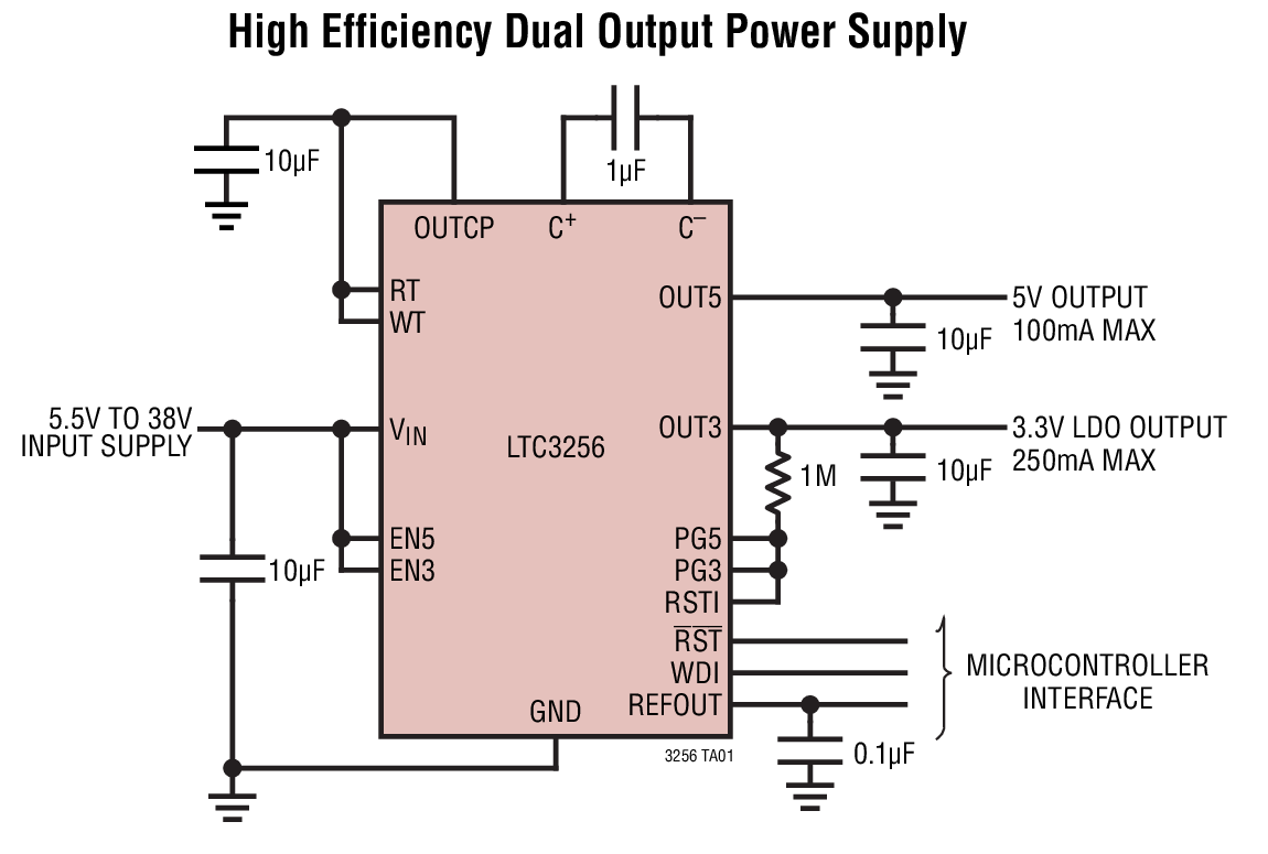
LTC3256 Demo Board | Dual Output Step-Down Charge Pump Plus LDO, 5.5V ≤ VIN ≤ 38V, VOUT1 = 5V @ 100mA, VOUT2 = 3.3V @ 250mA
Analog Devices Inc.
LTC3256 Demo Board | Dual Output Step-Down Charge Pump Plus LDO, 5.5V ≤ VIN ≤ 38V, VOUT1 = 5V @ 100mA, VOUT2 = 3.3V @ 250mA
Analog Devices Inc.
Demonstration Circuit 2375A is a dual output 350mA step down charge pump with a post-regulator LDO and watchdog timer featuring the LTC3256EMSE. The LTC3256 operates with a wide input voltage range from 5.5V to 38V and is engineered for diagnostic coverage in ISO262262 systems. The LTC3256 can provide up to 350mA of output current from a 12V battery with 2W less power dissipation than 2 ideal linear regulators. The DC2375A was populated with automotive grade components for evaluation. Because of the wide input operating range it is possible to exceed the specified operating junction temperature and even reach thermal shutdown with heavy loads. Please refer to the data sheet for additional information on the thermal limitations of the device.
Universal Line Power Supply for PLC using PSR Flyback and Compact DC/DC Stages Reference Design

Texas Instruments
Universal Line Power Supply for PLC using PSR Flyback and Compact DC/DC Stages Reference Design
Texas Instruments
The PMP9185 reference design uses the UCC28710 primary-side regulated flyback controller to generate a 15V output from a univeral AC input with maximum 20W output power followied by DC/DC and LDO stages using TPS54229 and TPS650250: and 5V: 3.3V: 1.8V and 1.2V are provided. A switch on the PCB provides the freedom of supplying DC/DC and LDO from AC input or DC input.
19 to 30Vin 12V@10A Active Clamp Forward Reference Design

Texas Instruments
19 to 30Vin 12V@10A Active Clamp Forward Reference Design
Texas Instruments
This reference design provides an isolated 12V at 10A from a 19V-30V input with greater than 93% efficiency. This design uses the UCC2897A active clamp controller with CSD18532Q5B synchronous rectifiers for an efficient: yet cost effective solution that can operate from a 24VDC input bus.
16…28V to21V/8.5A
Texas Instruments
16…28V to21V/8.5A
Texas Instruments
PMP2627 is a synchronous buck converter with 16-28V DC input voltage range. The output with 12.0V @ 8.5A has much output capacitance for big load steps. The converter resists voltage peaks up to 40V on the input and an input filter reduces ripple on the supply voltage rail.
Single-Channel Industrial Voltage & Current Output Driver: Isolated: EMC/EMI Tested Reference Design

Texas Instruments
Single-Channel Industrial Voltage & Current Output Driver: Isolated: EMC/EMI Tested Reference Design
Texas Instruments
This TI CerTIfied Reference Design implements a isolated single-channel industrial voltage and current output module using the DAC8760 and ISO7641. The circuit features a digitally controlled voltage or current output that produces the standard outputs of 0-20mA: 0-24mA: 4-20mA: 0-5V: +/-5V: 0-10V and +/-10V outputs based on the internal register settings of the DAC8760. The design includes the required external protection circuitry needed to pass the IEC61000-4-2/3/4/6 tests and IEC61000-4 test results are included. The protection circuitry does not negatively affect the voltage or current output performance resulting in
DC2548A

Analog Devices Inc.
DC2548A
Analog Devices Inc.
The LT8672 is an active rectifier controller for reverse input protection. It drives an external N-channel MOSFET to replace a power Schottky diode. Its very low quiescent current and fast transient response meet the tough requirements in automotive applications where AC input signals of up to 100kHz are present. These signals are rectified with minimum power dissipation on the external FET, simplifying thermal management on the PCB.With a drop of only 20mV, the LT8672 solution eases the minimum input voltage requirement during cold crank and start-stop, allowing simpler and more efficient circuits. If the input power source fails or is shorted, a fast turn-off minimizes reverse current transients. An available shutdown mode reduces the quiescent current to 3.5?A.An integrated auxiliary boost regulator provides the required boost voltage to turn the external FET fully on. A power good pin signals when the external FET is ready to take load current.Applications Automotive Battery Protection Industrial Supplies Portable Instrumentation
ADL5500-EVALZ

Analog Devices Inc.
ADL5500-EVALZ
Analog Devices Inc.
The ADL5500 is a mean-responding power detector for use in high frequency receiver and transmitter signal chains from 100 MHz to 6 GHz. It is easy to apply, requiring only a single supply between 2.7 V and 5.5 V and a power supply decoupling capacitor. The input is internally ac-coupled and has a nominal input impedance of 50 ?. The output is a linear-responding dc voltage with a conversion gain of 6.4 V/V rms at 900 MHz. The on-chip, 1 k? series resistance at the output combined with an external shunt capacitor creates a low-pass filter response that reduces the residual ripple in the dc output voltage.The ADL5500 is intended for true power measurement of simple and complex waveforms. The device is particularly useful for measuring high crest factor (high peak-to-rms ratio) signals, such as CDMA2000, W-CDMA, and QPSK/QAM-based OFDM waveforms.The ADL5500 offers excellent temperature stability with near 0 dB measurement error across temperature. The high accuracy range, centered around +3 dBm at 900 MHz, offers ?0.1 dB error from ?40?C to +85?C over an 8.5 dB range. The ADL5500 reduces calibration requirements with low drift across a 30 dB range over temperature and process variations.The ADL5500 operates from ?40?C to +85?C and is available in a 4-ball, 1.0 mm ? 1.0 mm wafer-level chip scale package. It is fabricated on a proprietary high fT silicon bipolar process.

Single-Ended Input to Differential Output Conversion Circuit Reference Design

Texas Instruments
Single-Ended Input to Differential Output Conversion Circuit Reference Design
Texas Instruments
This TI Precision Verified Design provides the theory: component selection: simulation: PCB design: and measurement details for a single ended input to differential output circuit which converts a single ended input of +0.1V to +2.4V into a differential output of ± 2.3V on a single +2.7V supply. The output range is intentionally limited to maximize linearity. The circuit is composed of 2 amplifiers. One amplifier acts as a buffer and creates a voltage: Vout+. The second amplifier inverts the input and adds a reference voltage to generate Vout-. Both Vout+ and Vout- range from 0.1V to 2.4V. The difference: Vdiff: is the difference between Vout+ and Vout-. This makes the differential output voltage range +2.3V.
DC2387A

Analog Devices Inc.
DC2387A
Analog Devices Inc.
The LTM8071 is a 60VIN, 5A (continuous) step-down Silent Switcher ?Module? (power module) regulator. The Silent Switcher architecture minimizes EMI while delivering high efficiency at frequencies up to 2.2MHz. Included in the package are the switching controller, power switches, inductor, and all support components. Operating over an input voltage range of 3.6V to 60V, the LTM8071 supports an output voltage range of 0.97V to 15V and a switching frequency range of 200kHz to 2.2MHz, each set by a single resistor. Only the input and output filter capacitors are needed to finish the design.The LTM8071 is packaged in a compact over-molded ball grid array (BGA) package suitable for automated assembly by standard surface mount equipment. The LTM8071 is available with SnPb (BGA) or RoHS compliant terminal finish.APPLICATIONS Test and Measurement Equipment Aviation Distributed Supply Regulation Industrial Supplies Wall Transformer Regulation
6V to 20V Synchronous Buck Controller with Sync and Power Good
Texas Instruments
6V to 20V Synchronous Buck Controller with Sync and Power Good
Texas Instruments
The design implements a TPS40195. The TPS40195 is a flexible synchronous buck controller that operates from a nominal 4.5 V to 20 V supply. This controller implements voltage mode control with the switching frequency adjustable from 100 kHz to 600 kHz. Flexible features found on this device include
Modeling Bi-Directional Buck/Boost Converter for Digital Control Using C2000 MCU
Texas Instruments
Modeling Bi-Directional Buck/Boost Converter for Digital Control Using C2000 MCU
Texas Instruments
This application report derives a unified model of a bi-directional buck boost converter in either mode of operation using state space averaging technique.
