
Search results
ADL5387-EVALZ

Analog Devices Inc.
ADL5387-EVALZ
Analog Devices Inc.
The ADL5387 is a broadband quadrature I/Q demodulator that covers an RF/IF input frequency range from 30 MHz to 2 GHz. With a NF = 13.2 dB, IP1dB = 12.7 dBm, and IIP3 = 32 dBm @ 450 MHz, the ADL5387 demodulator offers outstanding dynamic range suitable for the demanding infrastructure direct-conversion requirements. The differential RF/IF inputs provide a well-behaved broadband input impedance of 50 ? and are best driven from a 1:1 balun for optimum performance.Ultrabroadband operation is achieved with a divide-by-2 method for local oscillator (LO) quadrature generation. Over a wide range of LO levels, excellent demodulation accuracy is achieved with amplitude and phase balances ~0.05 dB and ~0.4?, respectively. The demodulated in-phase (I) and quadrature (Q) differential outputs are fully buffered and provide a voltage conversion gain of >4 dB. The buffered baseband outputs are capable of driving a 2 Vp-p differential signal into 200 ?.The fully balanced design minimizes effects from second-order distortion. The leakage from the LO port to the RF port is 60 dBm.The ADL5387 operates off a single 4.75 V to 5.25 V supply. The supply current is adjustable with an external resistor from the BIAS pin to ground.The ADL5387 is fabricated using the Analog Devices, Inc. advanced silicon-germanium bipolar process and is available in a 24-lead exposed paddle LFCSP.APPLICATIONS QAM/QPSK RF/IF demodulators W-CDMA/CDMA/CDMA2000/GSM Microwave point-to-(multi)point radios Broadband wireless and WiMAX Broadband CATVs
EVAL-AD7980SDZ

Analog Devices Inc.
EVAL-AD7980SDZ
Analog Devices Inc.
The AD7980 is a 16-bit, successive approximation, analog-to-digital converter (ADC) that operates from a single power supply, VDD. It contains a low power, high speed, 16-bit sampling ADC and a versatile serial interface port. On the CNV rising edge, it samples an analog input IN+ between 0 V to REF with respect to a ground sense IN?. The reference voltage, REF, is applied externally and can be set independent of the supply voltage, VDD. Its power scales linearly with throughput.The SPI-compatible serial interface also features the ability, using the SDI input, to daisy-chain several ADCs on a single, 3-wire bus and provides an optional busy indicator. It is compatible with 1.8 V, 2.5 V, 3 V, or 5 V logic, using the separate supply VIO.The AD7980 is housed in a 10-lead MSOP or a 10-lead QFN (LFCSP) with operation specified from ?40?C to +125?C.APPLICATIONSAutomated test equipmentData acquisition systemsMedical instrumentsMachine automation
Triple Rate SDI IP FPGA Resource Utilization on SDXILEVK/AES-EXP-SDI-G Ref Dsgn (Rev. A)

Texas Instruments
Triple Rate SDI IP FPGA Resource Utilization on SDXILEVK/AES-EXP-SDI-G Ref Dsgn (Rev. A)
Texas Instruments
Texas Instruments triple rate (SD/HD/3G) SDI demonstration board showcases the LMH0340 serializerLMH0341 deserializer LMH0344 equalizer LMH1981 sync separator LMH1982 clock generator withgenlock and the DS25CP104 cross-point switch. There are many advantages to using the TexasInstruments chipset that include superior performance reduced cost using inexpensive FPGAs such asthe Xilinx S
EVAL-AD5761RSDZ

Analog Devices Inc.
EVAL-AD5761RSDZ
Analog Devices Inc.
The AD5761R/AD5721R are single channel, 16-/12-bit serialinput, voltage output, digital-to-analog converters (DACs).They operate from single supply voltages from +4.75 V to+30 V or dual supply voltages from ?16.5 V to 0 V VSS and+4.75 V to +16.5 V VDD. The integrated output amplifier,reference buffer, and reference provide a very easy to use,universal solution.The devices offer guaranteed monotonicity, integral nonlinearity(INL) of ?2 LSB maximum, 35 nV/?Hz noise, and 7.5 ?s settlingtime on selected ranges.The AD5761R/AD5721R use a serial interface that operates atclock rates of up to 50 MHz and are compatible with DSP andmicrocontroller interface standards. Double buffering allows theasynchronous updating of the DAC output. The input codingis user-selectable twos complement or straight binary. Theasynchronous reset function resets all registers to their defaultstate. The output range is user selectable, via the RA[2:0] bitsin the control register.The devices available in a 3 mm ? 3 mm LFCSP package and a16-lead TSSOP package offer guaranteed specifications over the?40?C to +125?C industrial temperature range.Applications Industrial automation Instrumentation, data acquisition Open-/closed-loop servo control, process control Programmable logic controllers
LTM4705 | 20VIN, Dual 5A Step-Down DC/DC μModule Regulator

Analog Devices Inc.
LTM4705 | 20VIN, Dual 5A Step-Down DC/DC μModule Regulator
Analog Devices Inc.
Demonstration circuit 3051A features the LTM4705, a high efficiency dual 5A or single 10A μModule® DC/DC regulator in a compact and low profile 6.25mm × 7.5mm × 3.22mm BGA package. The LTM4705 can take 3.1V to 20V input and generate 0.6V to 5.5V output (stepdown only). The DC3051A demo board is designed to take 6VIN to 20VIN to dual 5A jumper selectable outputs. The board operates by default at a fixed 1MHz and can be synchronized from 1MHz to 3MHz via the MODE/SYNC pin. With its high switching frequency and current mode architecture, a fast transient response to line and load changes is possible without sacrificing stability. The DC3051A can be used in forced continuous mode or pulse-skipping mode for low noise, or in Burst Mode® operation for high efficiency at light loads. Please see the LTM4705 data sheet for more detailed information. It is recommended to read the data sheet for the LTM4705 prior to making any changes to the DC3051A.
ADRF5549-EVALZ

Analog Devices Inc.
ADRF5549-EVALZ
Analog Devices Inc.
The ADRF5549 is a dual-channel, integrated, RF front-end multichip module designed for time division duplexing (TDD) applications that operates from 1.8 GHz to 2.8 GHz. The ADRF5549 is configured in dual channels with a cascading, two-stage, low noise amplifier (LNA) and a high power, silicon single-pole, double-throw (SPDT) switch.In high gain mode, the cascaded two-stage LNA and switch offer a low noise figure of 1.4 dB and a high gain of 35 dB with an output third-order intercept point (OIP3) of 32 dBm typical.In low gain mode, one stage of the two-stage LNA is in bypass mode providing 17 dB of gain at a lower current of 35 mA. In power-down mode, the LNAs are turned off, and the device draws 12 mA.In transmit operation, when RF inputs are connected to a termination pin (TERM-ChA or TERM-ChB), the switch provides a low insertion loss of 0.6 dB and handles a long-term evolution (LTE) full lifetime average (9 dB peak to average ratio (PAR)) of 40 dBm and 43 dBm for a 9 dB PAR LTE single event (ApplicationsWireless InfrastructureTDD massive multiple input and multiple output (MIMO) and active antenna systemsTDD-based communication systems
LT3754EUH Demo Board | 16-Channel Boost LED Driver, 20V ≤ VIN ≤ 28V, VLED = 55V @ 50mA

Analog Devices Inc.
LT3754EUH Demo Board | 16-Channel Boost LED Driver, 20V ≤ VIN ≤ 28V, VLED = 55V @ 50mA
Analog Devices Inc.
DC1436A is a 16-Channel High Voltage Boost LED Driver featuring the LT3754. The LT3754 drives up to 50mA per string and has a maximum LED string voltage of 45V. The VIN terminal is powered from an 8V to 14V input supply and is distinct from the 24V PVIN supply (20V to 28V) for best thermal performance. Overvoltage protection is set at 55V in case the LEDs are removed from the circuit. If the LEDs are opened, the FAULT terminal output flag goes low and reports the fault condition. If one or more of the 16 LED channels is not used, its LED pin or terminal should be tied to VOUT (LED+) to disable it. Multiple channels can be tied in parallel by tying their LED1-LED16 pins together.

ERA-6AEB6492V
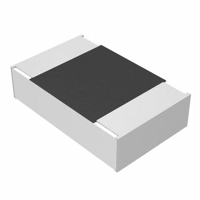
Panasonic Industrial Devices
From -$1.00 • 10 k+ units available from multiple sources
ERA-6AEB6492V
Panasonic Industrial Devices
ERA Series 0805 64.9 kOhm ?0.1% 0.125 W ?25 ppm/?C Thin Film Chip Resistor
| Distributor | SKU | Stock | MOQ | 1 | 10 | 50 | 100 | 1,000 | 10,000 | |
|---|---|---|---|---|---|---|---|---|---|---|
| DigiKey | P64.9KDACT-ND | 5,607 | 1 | $0.31 | $0.26 | $0.26 | $0.10 | $0.04 | $0.03 | |
| Mouser Electronics | 667-ERA-6AEB6492V | 4,997 | 1 | $0.35 | $0.30 | $0.30 | $0.12 | $0.05 | $0.04 | |
| Future Electronics | ERA-6AEB6492V | 5,000 | 5,000 | $0.04 | Buy |
Interfacing the TLC4541 to TMS320C6711 DSP
Texas Instruments
Interfacing the TLC4541 to TMS320C6711 DSP
Texas Instruments
This application note presents a method for interfacing the TLC4541 16-bit SAR analog-to-digital converter to the TMS320C6711™ DSP McBSP1. The software developed reads 1024 samples continuously from the TLC4541. In an effort to reduce development time the source code is made available on TI's website.
DC2966A

Analog Devices Inc.
DC2966A
Analog Devices Inc.
The LTC3376 is a highly flexible multioutput power supply IC. The device includes four synchronous buck converters, configured to share eight 1.5A power stages, powered from independent 3V to 20V inputs. The DC/DCs are assigned to one of fifteen power configurations via pin strappable CFG0 to CFG3 pins. The LTC3376 includes the integration of ceramic capacitors into the package for the BST pins thereby saving PCB space. The common buck switching frequency may be programmed with an external resistor, synchronized to an external oscillator, or set to a default internal 2MHz clock. The operating mode for all DC/DCs may be programmed via the SYNC/MODE pin for Burst Mode or forced continuous mode operation. The PGOOD1 to PGOOD4 outputs indicate when each enabled DC/DC is within a specified percentage of its final output. Current monitors allow for external monitoring of each buck?s load. The EXTVCC pin allows for the internal circuitry to run from a 3V to 5.5V rail for improved efficiency. Precision RUN pin thresholds facilitate power-up sequencing. The LTC3376 is available in a 64 lead 7mm ? 7mm BGA (0.8mm ball pitch).Applications? Telecom/Industrial? 12V Distributed Power Systems
EVAL-AD4114SDZ

Analog Devices Inc.
EVAL-AD4114SDZ
Analog Devices Inc.
The AD4114 is a low power, low noise, 24-bit, sigma-delta (?-?) analog-to-digital converter (ADC) that integrates an analog front end (AFE) for eight fully differential or 16 single-ended, high impedance (?1 M?), bipolar, ?10 V voltage inputs.The AD4114 integrates key analog and digital signal conditioning blocks to configure eight individual setups for each analog input channel in use. The AD4114 features a maximum channel scan rate of 6.21 kSPS (161 ?s) for fully settled data.The embedded 2.5 V, low drift (?5 ppm/?C), band gap internal reference (with output reference buffer) reduces the external component count.The digital filter allows flexible settings, including simultaneous 50 Hz and 60 Hz rejection at a 27.27 SPS output data rate. The user can select different filter settings depending on the requirements of each channel in the application. The automatic channel sequencer enables the ADC to switch through each enabled channel.The precision performance of the AD4114 is achieved by integrating the proprietary iPassives? technology from Analog Devices, Inc. The AD4114 is factory calibrated to achieve a high degree of specified accuracy.The AD4114 operates with a single power supply that allows simplified use in galvanically isolated applications. The specified operating temperature range is ?40?C to +105?C. The AD4114 is housed in a 40-lead, 6 mm ? 6 mm LFCSP.ApplicationsProgrammable logic controller (PLC) and distributed control system (DCS) modules Instrumentation and measurement
Compensation Made SIMPLE With LM4360x, LM4600x
Texas Instruments
Compensation Made SIMPLE With LM4360x, LM4600x
Texas Instruments
Compensating a DC-DC buck converter is challenging if the designer is not familiar with the loop control theory. To achieve a stable design under all corner and adverse conditions, the user must prope
Dynamic Near Field Communication (NFC) Type 4B Tag

Texas Instruments
Dynamic Near Field Communication (NFC) Type 4B Tag
Texas Instruments
This dynamic Near Field Communication (NFC) tag design outlines the required components: layout considerations: and provides firmware examples to implement NFC into applications such as Bluetooth® and Wi-Fi® pairing: equipment configuration and diagnostics: or as a general purpose NFC data interface. The documentation: hardware: and example code provided allows the designer to quickly implement NFC functionality with an MSP430 or other MCU of choice.