
Search results
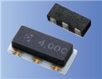
EASV2110BA3

Everlight
From $0.04 • 1 k+ units available from multiple sources
| Distributor | SKU | Stock | MOQ | 1 | 10 | 50 | 100 | 1,000 | 10,000 | |
|---|---|---|---|---|---|---|---|---|---|---|
| DigiKey | EASV2110BA3-ND | 0 | 9,000 | $0.06 | Buy | |||||
| Mouser Electronics | N/A | 0 | ||||||||
| AVNET Express | EASV2110BA3 | 3,000 | 3,000 | $0.06 | Buy | |||||
| Arrow North American Components | EASV2110BA3 | 0 | 9,000 | $0.06 | $0.21 | $0.13 | $0.11 | $0.04 | $0.04 | |
| Verical Marketplace | EASV2110BA3 | 3,000 | 180 | $0.04 | $0.04 |
CGJ3E2X7R1C154K080AA
TDK Corporation
From $0.12 • 10 k+ units available from Quarktwin Electronic Components
CGJ3E2X7R1C154K080AA
TDK Corporation
Cap Ceramic 0.15uF 16V X7R 10% SMD 0603 125°C Punched Paper T/R
| Distributor | SKU | Stock | MOQ | 1 | 10 | 50 | 100 | 1,000 | 10,000 | |
|---|---|---|---|---|---|---|---|---|---|---|
| DigiKey | 445-13339-1-ND | 0 | 1 | |||||||
| AVNET Express | CGJ3E2X7R1C154K080AA | 0 | 4,000 | Buy | ||||||
| Newark | CGJ3E2X7R1C154K080AA | 0 | 4,000 | $0.00 | $0.00 | $0.00 | $0.00 | $0.00 | $0.00 | Buy |
| Ameya360 | CGJ3E2X7R1C154K080AA | 4,000 | Buy | |||||||
| Quarktwin Electronic Components | CGJ3E2X7R1C154K080AA | 19,836 | 10 | $0.20 | $0.18 | $0.18 | $0.16 | $0.13 | $0.12 | Buy |
ADL8150-EVALZ

Analog Devices Inc.
ADL8150-EVALZ
Analog Devices Inc.
The ADL8150 is a self biased gallium arsenide (GaAs), monolithic microwave integrated circuit (MMIC), heterojunction bipolar transistor (HBT), low phase noise amplifier that operates from 6 GHz to 14 GHz. The amplifier provides 12 dB of typical signal gain, 18 dBm output power at 1 dB gain compression (OP1dB), and a typical output third-order intercept (OIP3) of 30 dBm. The amplifier requires 74 mA from a 5 V collector supply voltage. The ADL8150 also features inputs and outputs (I/Os) that are internally matched to 50 ?, and facilitates integration into multichip modules (MCMs). Note that throughout the data sheet, multifunction pins, such as RFOUT/VCC, are referred to either by the entire pin name or by a single function of the pin, for example, RFOUT, when only that function is relevant.Applications Military and space Test instrumentation Communications
ADRF5549-EVALZ

Analog Devices Inc.
ADRF5549-EVALZ
Analog Devices Inc.
The ADRF5549 is a dual-channel, integrated, RF front-end multichip module designed for time division duplexing (TDD) applications that operates from 1.8 GHz to 2.8 GHz. The ADRF5549 is configured in dual channels with a cascading, two-stage, low noise amplifier (LNA) and a high power, silicon single-pole, double-throw (SPDT) switch.In high gain mode, the cascaded two-stage LNA and switch offer a low noise figure of 1.4 dB and a high gain of 35 dB with an output third-order intercept point (OIP3) of 32 dBm typical.In low gain mode, one stage of the two-stage LNA is in bypass mode providing 17 dB of gain at a lower current of 35 mA. In power-down mode, the LNAs are turned off, and the device draws 12 mA.In transmit operation, when RF inputs are connected to a termination pin (TERM-ChA or TERM-ChB), the switch provides a low insertion loss of 0.6 dB and handles a long-term evolution (LTE) full lifetime average (9 dB peak to average ratio (PAR)) of 40 dBm and 43 dBm for a 9 dB PAR LTE single event (ApplicationsWireless InfrastructureTDD massive multiple input and multiple output (MIMO) and active antenna systemsTDD-based communication systems
DC2019B

Analog Devices Inc.
DC2019B
Analog Devices Inc.
The LT8614 step-down regulator features Silent Switcher architecture designed to minimize EMI emissions while delivering high efficiency at frequencies up to 3MHz. Assembled in a 3mm ? 4mm QFN, the monolithic construction with integrated power switches and inclusion of all necessary circuitry yields a solution with a minimal PCB footprint. An ultralow 2.5?A quiescent current?with the output in full regulation? enables applications requiring highest efficiency at very small load currents. Transient response remains excellent and output voltage ripple is below 10mVP-P at any load, from zero to full current.The LT8614 allows high VIN to low VOUT conversion at high frequency with a fast minimum top switch on-time of 30ns. Operation is safe in overload even with a saturated inductor.Essential features are included and easy to use: An open-drain PG pin signals when the output is in regulation. The SYNC pin allows clock synchronization and choice of Burst Mode operation or pulse-skipping mode. Soft-start and tracking functionality is accessed via the TR/SS pin. An accurate enable threshold can be set using the EN/UV pin and a resistor at the RT pin programs switch frequency.Applications Automotive and Industrial Supplies General Purpose Step-Down GSM Power Supplies
Comparator with Hysteresis Reference Design

Texas Instruments
Comparator with Hysteresis Reference Design
Texas Instruments
This TI Verified Design implements a comparator with hysteresis. Comparators are used to differentiate between two different signal levels. For example: a comparator may differentiate between an over temperature and normal temperature condition. Noise or signal variation at the comparison threshold will cause multiple transitions. Hysteresis sets an upper and lower threshold to eliminate the multiple transitions caused by noise.
1mW Converter: 3.1V @ 300uA

Texas Instruments
1mW Converter: 3.1V @ 300uA
Texas Instruments
The PMP7022 is 1mW (3.1V at 300uA) galvanic isolated DC/DC reference design built to supply a MSP430 metering unit. The design utilising again MSP430 open loop push-pull stage. Very efficient design with current supply (inclusive load current) as low as 800uA. Input voltage range: 3.1VDC-3.3VDC; Output current: 300uA; Output voltage: 3.1VDC
6 to 16Vin 12V@4A Output Wide Vin SEPIC Converter Reference Design

Texas Instruments
6 to 16Vin 12V@4A Output Wide Vin SEPIC Converter Reference Design
Texas Instruments
This is a Wide-Vin SEPIC converter with an operating input voltage range of 6V to 16V: and implements an output of 12V with the capability of supplying 4A of current to load.
ADMV1013-EVALZ

Analog Devices Inc.
ADMV1013-EVALZ
Analog Devices Inc.
The ADMV1013 is a wideband, microwave upconverter optimized for point to point microwave radio designs operating in the 24 GHz to 44 GHz radio frequency (RF) range.The upconverter offers two modes of frequency translation. The device is capable of direct conversion to RF from baseband in-phase quadrature (I/Q) input signals, as well as single-sideband (SSB) upconversion from complex intermediate frequency (IF) inputs. The baseband I/Q input path can be disabled and modulated complex IF signals, anywhere from 0.8 GHz to 6.0 GHz, can be inserted in the IF path and upconverted to 24 GHz to 44 GHz while suppressing the unwanted sideband by typically better than 26 dBc. The serial port interface (SPI) allows adjustment of the quadrature phase and mixer gate voltage to allow optimum sideband suppression and local oscillator (LO) nulling. In addition, the SPI interface allows powering down the output envelope detector to reduce power consumption.The ADMV1013 upconverter comes in a 40-terminal land grid array package (LGA) package. The ADMV1013 operates over the ?40?C to +85?C case temperature range.Applications Point to point microwave radios Radar, electronic warfare systems Instrumentation, automatic test equipment (ATE)
LTC3634EUFD Demo Board (QFN) | VIN= 3.6V to 15V, VOUT1 =1.5V/1.8V/2.5V@±3A, VOUT2 = 0.5VIN (VTT)@±3A, VOUT3 = 0.5VIN (VTTR)@±10mA

Analog Devices Inc.
LTC3634EUFD Demo Board (QFN) | VIN= 3.6V to 15V, VOUT1 =1.5V/1.8V/2.5V@±3A, VOUT2 = 0.5VIN (VTT)@±3A, VOUT3 = 0.5VIN (VTTR)@±10mA
Analog Devices Inc.
Demonstration circuit DC1708A is a dual-output regulator focused specifically for DDR memory power applications. It is built based on the LTC3634, a high voltage dualchannel, controlled on-time monolithic synchronous buck regulator. The DC1708A has an input voltage range of 3.6V to 15V. The output voltage of the first channel, VDDQ, of the DC1708A has three fixed voltage settings: 1.5V, 1.8V and 2.5V, and is capable of delivering up to 3A of output current. The second channel, VTT, is set to regulate to half the voltage on the VDDQIN pin, which can be either the channel 1 output or an external reference voltage. It can source or sink a maximum of 3A of output current. The LTC3634 also provides a 10mA buffered output of half VDDQIN – VTTR, which is used to provide the reference voltage needed for DDR applications. With the use of a timing resistor, the DC1708A can have its operating frequency programmed from 500kHz to 4MHz. Additionally the DC1708A can be easily synchronized to an external clock, due to an internal phase-locked loop, within this same frequency range. The DC1708A VDDQ output can operate in either Burst Mode® operation or forced continuous mode. In Burst Mode operation, which is the preferred mode of low load current operation, the DC supply current is typically only 1.3mA (both channels) at no load (sleep mode), and less than 15µA in shutdown. In Burst Mode operation or continuous mode operation, the DC1708A is a very efficient circuit at high load currents: over 80% for either channel. The LTC3634 is also capable of 90° or 180° out-of-phase operation, and can allow its output to track an external voltage, either coincidentally or ratiometrically. The LTC3634 comes in a 28-pin QFN package, featuring an exposed pad on the bottom-side of the IC for better thermal performance. All of these features make the DC1708A an ideal circuit for powering DDR memory applications.
AN-2052 Texas Instruments SIMPLE SWITCHER Power Modules and EMI (Rev. C)
Texas Instruments
AN-2052 Texas Instruments SIMPLE SWITCHER Power Modules and EMI (Rev. C)
Texas Instruments
While the principles discussed in this application report apply more broadly to power design we will focuson DC to DC convertor design given its broad application. It affects virtually every hardware engineer whoat some point has to design a power convertor. In this application report we will consider two commontrade-offs related to low EMI design; thermal performance and EMI and also solut
Using UCC25710 to design cost effective LED Power

Texas Instruments
Using UCC25710 to design cost effective LED Power
Texas Instruments
PMP6252 is a reference design for 90W LCD TV power by using the UCC28051 to construct PFC: UCC25710 to construct LED driver LLC converter: UCC25600 to construct 5V and 12V converter and UCC28610 to construct standby flyback converter. This driver provides 4 outputs including LED driver: 12.7V 3A: 5V 3A and 5V standby 2A; and has the capability to operate at 90~264Vac.The LED driver is designed using multi-transformer topology by UCC25710 which can improve efficiency: has protection function and decrease component count. A thorough analysis of PFC: LLC: cascade QR flyback operation and performance along with design optimization guidelines are presented. Experimental results obtained on every general condition load are provided.
ADP2114-2PH-EVALZ
Analog Devices Inc.
From $92.96 • 1 unit available from Verical Marketplace
ADP2114-2PH-EVALZ
Analog Devices Inc.
Configurable, Dual 2 A/Single 4 A, Synchronous Step-Down DC-to-DC Regulator Features: Configurable 3 A/1 A or 2 A/2 A dual output load combinations or 4 A combined single output High efficiency: up to 95% Input voltage VIN: 2.75 V to 5.5 V Selectable fixed output: 0.8 V, 1.2 V, 1.5 V, 1.8 V, 2.5 V, 3.3 V or adjustable output voltage to 0.6 V minimum ±1.5% accuracy reference voltage Selectable fixed switching frequency: 300 kHz, 600 kHz, or 1.2 MHz Optimized gate slew rate for reduced EMI External synchronization or internal clock output Dual-phase, 180° shifted PWM channels Current mode for fast transient response, no current sense resistor required Pulse-skip under light load or forced PWM operation See data sheet for additonal features
| Distributor | SKU | Stock | MOQ | 1 | 10 | 50 | 100 | 1,000 | 10,000 | |
|---|---|---|---|---|---|---|---|---|---|---|
| DigiKey | ADP2114-2PH-EVALZ-ND | 0 | 1 | $89.27 | $89.27 | $89.27 | $89.27 | $89.27 | $89.27 | Buy |
| Mouser Electronics | 584-ADP2114-2PHEVALZ | 0 | 1 | $75.65 | $75.65 | $75.65 | $75.65 | $75.65 | $75.65 | |
| Newark | ADP2114-2PH-EVALZ | 0 | $77.25 | $77.25 | $77.25 | $77.25 | $77.25 | $77.25 | Buy | |
| Arrow North American Components | ADP2114-2PH-EVALZ | 0 | 1 | $74.56 | $74.56 | $74.56 | $74.56 | $74.56 | $74.56 | |
| Verical Marketplace | ADP2114-2PH-EVALZ | 1 | 1 | $92.96 | $92.96 | $92.96 | $92.96 | $92.96 | $92.96 | |
| Analog Devices Inc | ADP2114-2PH-EVALZ | 0 | $66.12 | $66.12 | $66.12 | $66.12 | $66.12 | $66.12 | Buy |
EVAL-ADAQ23876FMCZ

Analog Devices Inc.
EVAL-ADAQ23876FMCZ
Analog Devices Inc.
The ADAQ23876 is a precision, high speed, ?Module? data acquisition solution that reduces the development cycle of a precision measurement systems by transferring the design burden of component selection, optimization, and layout from the designer to the device.Using System-in-Package (SIP) technology, the ADAQ23876 reduces end system component count by combining multiple common signal processing and conditioning blocks in a single device, including a low noise, fully differential ADC driver (FDA), a stable reference buffer, and a high speed, 16-bit, 15 MSPS successive approximation register (SAR) ADC.The ADAQ23876 also incorporates the critical passive components with superior matching and drift characteristics using Analog Devices, Inc., iPassive? technology to minimize temperature dependent error sources and to offer optimized performance. The fast settling of the ADC driver stage and no latency of the SAR ADC provide a unique solution for high channel count multiplexed signal chain architectures and control loop applications.The small footprint, 9 mm ? 9 mm BGA package enables smaller form factor instruments without sacrificing performance. The system integration solves many design challenges while the device still provides the flexibility of a configurable ADC driver feedback loop to allow gain or attenuation adjustments, as well as fully differential or single-ended to differential input. A single 5 V supply operation is possible while achieving optimum performance from the device.The ADAQ23876 features a serial LVDS digital interface with one-lane or two-lane output modes, allowing the user to optimize the interface data rate for each application. The specified operation of the ?Module is from ?40?C to +85?C.APPLICATIONS Automatic test equipment Data acquisition Hardware in the Loop (HiL) Power analyzers Nondestructive test (acoustic emissions) Mass spectrometry Traveling wave fault location Medical imaging and instruments?