
Search results
Ceramic Capacitors Replace Tantalum Capacitors in LDOs (Rev. A)

Texas Instruments
Ceramic Capacitors Replace Tantalum Capacitors in LDOs (Rev. A)
Texas Instruments
With the proper considerations ceramic output capacitors can be used with low dropout regulators (LDO) and DC/DC switching converters that require tantulum output capacitors.
Using the AM17xx Bootloader (Rev. C)
Texas Instruments
Using the AM17xx Bootloader (Rev. C)
Texas Instruments
This application report describes various boot mechanisms supported by the AM17xx bootloader read-only memory (ROM) image. Topics covered include the Application Image Script (AIS) boot process an AISgen tool used to generate boot scripts protocol for booting the device from an external master device a UART Boot Host GUI for booting the device from a host PC and any limitations default settin
Booting a TMS320C32 Target System in a C Environment
Texas Instruments
Booting a TMS320C32 Target System in a C Environment
Texas Instruments
TI supports four methods of booting a 32-bit floating point DSP following system reset. Each method uses a different combination of the TMS320C32 silicon features software and hardware tools. Each combination forms an integrated development environment that includes features to support most system boot requirements. This document describes in detail the four methods of system boot and provid
Design Considerations for the UCC28600 (Rev. B)
Texas Instruments
Design Considerations for the UCC28600 (Rev. B)
Texas Instruments
The UCC28600 Quasi-Resonant Green-Mode Controller provides engineers with a cost-effective solution for designing energy efficient power supplies. Despite the 8-pin package the device has many built-in advanced protection features. Because most of the pins on the device have dual functions careful attention must be given to the design and layout of the circuit. What follows is a brief discuss
Implementing Continuously Programmable Digital Filters w/ TMS320C30/40 DSP (Rev. A)
Texas Instruments
Implementing Continuously Programmable Digital Filters w/ TMS320C30/40 DSP (Rev. A)
Texas Instruments
Systems engineers must apply real-time digital hardware solutions to signal processing problems to achieve the goals of reliability repeatability and flexibility. DSP offers the only such solution for many applications. Digital filter components are an integral part of many DSP systems. In particular continuously programmable digital filters (CPDFs) offer a broad range of high-tech applicatio
AD8334-EVALZ

Analog Devices Inc.
AD8334-EVALZ
Analog Devices Inc.
The AD8334 is an ultralow noise, quad channel linear-in-dB variable gain amplifier (VGA). Although optimized for ultrasound systems, it may be used as a low noise variable gain control in any application whose operating frequency is less than 100 MHz.Included in each channel are an ultralow noise preamp (LNA), an X-AMP? VGA with 48 dB of gain range, and a selectable gain postamp with adjustable output limiting. The LNA gain is 19 dB with a single-ended input and differential outputs. Using a single resistor, the LNA input impedance can be adjusted to match a signal source without compromising noise performance.The 48 dB gain range of the VGA makes these devices suitable for a variety of applications. Excellent bandwidth uniformity is maintained across the entire range. The gain control interface provides precise linear-in-dB scaling of 50 dB/V for control voltages between 40 mV and 1 V. Factory trim ensures excellent part-to-part and channel-to-channel gain matching. Differential signal paths result in superb second- and third-order distortion performance and low crosstalk.The AD8334 is a quad version of the single AD8331 and dual AD8332.For information on specs, see the AD8331/AD8332/AD8334 datasheet.Applications Ultrasound and sonar time-gain controls High performance automatic gain control (AGC) systems I/Q signal processing High speed, dual ADC drivers
What is a .tmap File? (Rev. A)
Texas Instruments
What is a .tmap File? (Rev. A)
Texas Instruments
The PowerLAN™ Master Gateway Battery Management Controller uses a file identified by the .tmap file extension to load configuration parameters. This file serves to configure the operation of the controller to the specific application. Examples of configurable parameters are number of parallel and series cells in the pack number of temperature sensors and state-of-charge indication (SOCi) dis
EVAL-AD4003FMCZ

Analog Devices Inc.
EVAL-AD4003FMCZ
Analog Devices Inc.
The AD4003/AD4007/AD4011 are high accuracy, high speed, low power, 18-bit, Easy Drive, precision successive approximation register (SAR) analog-to-digital converters (ADCs) that operate from a single power supply, VDD. The reference voltage, VREF, is applied externally and can be set independent of the supply voltage. The AD4003/AD4007/AD4011 power scales linearly with throughput. Easy Drive features reduce both signal chain complexity and power consumption while enabling higher channel density. The reduced input current, particularly in high-Z mode, coupled with a long signal acquisition phase, eliminates the need for a dedicated ADC driver. Easy Drive broadens the range of companion circuitry that is capable of driving these ADCs (see Figure 2 in the data sheet).Input span compression eliminates the need to provide a negative supply to the ADC driver amplifier while preserving access to the full ADC code range. The input overvoltage clamp protects the ADC inputs against overvoltage events, minimizing disturbances on the reference pin and eliminating the need for external protection diodes. Fast device throughput up to 2 MSPS allows users to accurately capture high frequency signals and to implement oversampling techniques to alleviate the challenges associated with antialias filter designs. Decreased serial peripheral interface (SPI) clock rate requirements reduce digital input and output power consumption, broadens digital host options, and simplifies the task of sending data across digital isolation. The SPI-compatible serial user interface is compatible with 1.8 V, 2.5 V, 3 V, and 5 V logic by using the separate VIO logic supply.APPLICATIONS Automated test equipment Machine automation Medical equipment Battery-powered equipment Precision data acquisition systems Instrumentation and control systems
AD9228-65KITZ
Analog Devices Inc.
AD9228-65KITZ
Analog Devices Inc.
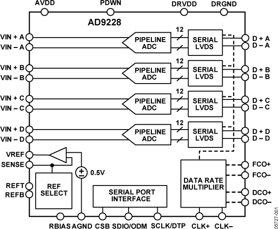
The AD9228 is a quad, 12-bit, 40/65 MSPS analog-to-digital converter (ADC) with an on-chip sample-and-hold circuit designed for low cost, low power, small size, and ease of use. The product operates at a conversion rate of up to 65 MSPS and is optimized for outstanding dynamic performance and low power in applications where a small package size is critical. The ADC requires a single 1.8 V power supply and LVPECL-/ CMOS-/LVDS-compatible sample rate clock for full performance operation. No external reference or driver components are required for many applications. The ADC automatically multiplies the sample rate clock for the appropriate LVDS serial data rate. A data clock output (DCO) for capturing data on the output and a frame clock output (FCO) for signaling a new output byte are provided. Individual channel power-down is supported and typically consumes The ADC contains several features designed to maximize flexibility and minimize system cost, such as programmable clock and data alignment and programmable digital test pattern generation. The available digital test patterns include built-in deterministic and pseudorandom patterns, along with custom user-defined test patterns entered via the serial port interface (SPI). The AD9228 is available in an RoHS compliant, 48-lead LFCSP. It is specified over the industrial temperature range of ?40?C to +85?C.PRODUCT HIGHLIGHTSSmall Footprint. Four ADCs are contained in a small, space-saving package. Low power of 119 mW/channel at 65 MSPS. Ease of Use. A data clock output (DCO) is provided that operates at frequencies of up to 390 MHz and supports double data rate (DDR) operation.User Flexibility. The SPI control offers a wide range of flexible features to meet specific system requirements. Pin-Compatible Family. This includes the AD9287 (8-bit), AD9219 (10-bit), and AD9259 (14-bit).?APPLICATIONSMedical imaging and nondestructive ultrasound Portable ultrasound and digital beam-forming systemsQuadrature radio receivers Diversity radio receivers Tape drives Optical networking Test equipment
AD7134 Evaluation Board
Analog Devices Inc.
AD7134 Evaluation Board
Analog Devices Inc.
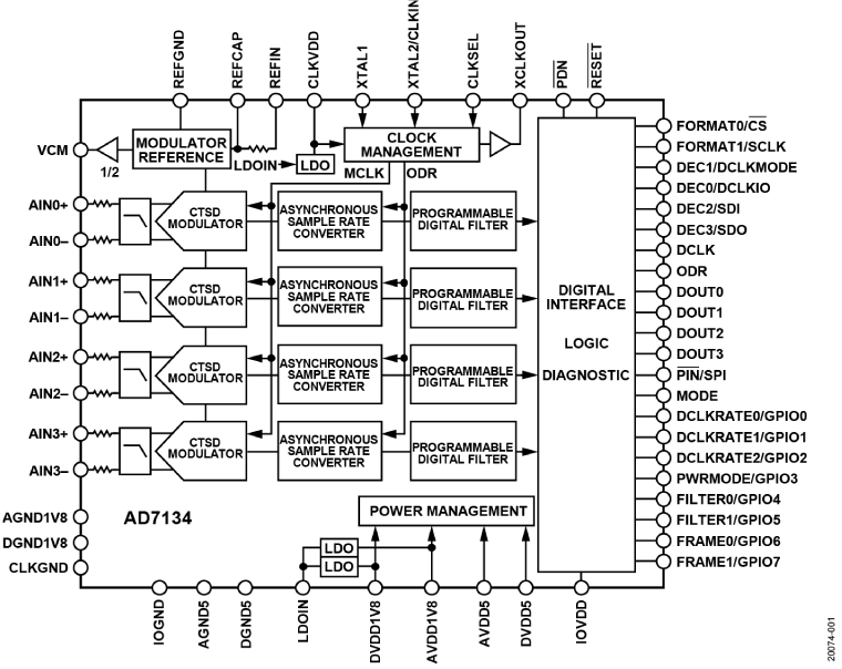
The EVAL-AD7134FMCZ evaluation kit features the AD7134 24-bit, 4-channel, simultaneous sampling, 1.5 MSPS precision alias free analog-to-digital converter (ADC). Two on-board AD7134 ADCs are included to demonstrate multidevice simultaneous sampling. The EVAL-AD7134FMCZ draws power from the system demonstration platform (SDP) EVAL-SDP-CH1Z (SDP-H1) board, and the on-board dc-to-dc regulators regulate an external supply of 8 V to 14 V down to 5 V, 1.8 V, and 1.2 V to supply the AD7134 and peripheral components. Both on-board ADCs have a separate reference of 4.096 V generated by the on-board ADR444. The ADCs have three clock input options and can be clocked by a crystal input, a microelectromechanical system (MEMS) oscillator, or a complementary metal-oxide semiconductor (CMOS) clock. The EVAL-AD7134FMCZ connects to the PC USB port via the SDP-H1 board. The AD7134 evaluation software running on a PC provides full accessibility to the AD7134 device register map, as well as a data analysis interface to display key parameters and graphics from the conversion result in both time and frequency domains. For full details on the AD7134, see the AD7134 data sheet, which must be consulted in conjunction with this user guide when using the EVAL-AD7134FMCZ.
ADL5390-EVALZ

Analog Devices Inc.
ADL5390-EVALZ
Analog Devices Inc.
The ADL5390 vector multiplier consists of a matched pair of broadband variable gain amplifiers whose outputs are summed. The separate gain controls for each amplifier are linear-in-magnitude. If the two input RF signals are in quadrature, the vector multiplier can be configured as a vector modulator or as a variable attenuator/phase shifter by using the gain control pins as Cartesian variables. In this case, the output amplitude can be controlled from a maximum of +5 dB to less than -30 dB, and the phase can be shifted continuously over the entire 360? range. Since the signal paths are linear, the original modulation on the inputs is preserved. If the two signals are independent, then the vector multiplier can function as a 2:1 multiplexer or can provide fading from one channel to another.The ADL5390 operates over a wide frequency range of 20 MHz to 2400 MHz. For a maximum gain setting on one channel at 380 MHz, the ADL5390 delivers an OP1dB of 11 dBm, an OIP3 of 24 dBm, and an output noise floor of -148 dBm/Hz. The gain and phase matching between the two VGAs is better than 0.5 dB and 1?, respectively, over most of the operating range.The ADL5390 is fabricated on Analog Devices' proprietary, high performance 25 GHz SOI complementary bipolar IC process. It is available in a 24-lead, Pb-free CSP package and operates over a -40?C to +85?C temperature range. Evaluation boards are available.APPLICATIONS PA linearization and predistortion Amplitude and phase modulation Variable matched attenuator and/or phase shifter Cellular base stations Radio links Fixed wireless access Broadband/CATV RF/IF analog multiplexerAVAILABILITYSamples, part number ADL5390ACPZ, and an evaluation board, part number ADL5390-EVAL, are available.COMPANION PRODUCTSAD8302 - LF to 2.7GHz RF/IF Gain Phase DetectorAD8340 - RF Vector Modulator 700MHz to 1000MHzAD8341 - RF Vector Modulator 1.5GHz to 2.4GHz
Synchronization Of ISO120/121 Isolation Amplifier
Texas Instruments
Synchronization Of ISO120/121 Isolation Amplifier
Texas Instruments
Internal clock circuitry in the ISO120/121 precision isolation amplifier (ISO amp) can be synchronized to an external clock signal. Synchronization to an external clock can be used to eliminate beat frequencies in multichannel systems or for rejection of specific AC signals and their harmonics.
EVAL-AD5320DBZ

Analog Devices Inc.
EVAL-AD5320DBZ
Analog Devices Inc.
The AD5320 is a single, 12-bit buffered voltage out DAC that operates from a single +2.7 V to +5.5 V supply consuming 115 ?A at 3 V. Its on-chip precision output amplifier allows rail-to-rail output swing to be achieved. The AD5320 utilizes a versatile three-wire serial interface that operates at clock rates up to 30 MHz and is compatible with standard SPI?,QSPI?, MICROWIRE? and DSP interface standards.The reference for AD5320 is derived from the power supplyinputs and thus gives the widest dynamic output range. Thepart incorporates a power-on reset circuit that ensures that theDAC output powers up to zero volts and remains there until avalid write takes place to the device. The part contains a power-down feature that reduces the current consumption of thedevice to 200 nA at 5 V and provides software selectable outputloads while in power-down mode. The part is put into power-down mode over the serial interface. The low power consumption of this part in normal operationmakes it ideally suited to portable, battery-operated equipment.The power consumption is 0.7 mW at 5 V reducing to 1 ?W inpower-down mode.The AD5320 is one of a family of pin-compatible DACs. TheAD5300 is the 8-bit version and the AD5310 is the 10-bitversion. The AD5300/AD5310/AD5320 are available in 6-leadSOT-23 packages and 8-lead MSOP packages. PRODUCT HIGHLIGHTS Available in 6-lead SOT-23 and 8-lead MicroSOIC packages Low power, single supply operation from 2.7 V to 5.5 V Consumes 0.35 mW at 3 V and 0.7 mW at 5 V Rail-to-Rail output with a slew rate of 1 V/?s Reference derived from the power supply High speed serial interface with clock speeds up to 30 MHz Pin and Software Compatible with the AD5300 (8-Bit) and the AD5310 (10-bit)APPLICATIONS Portable battery-powered instruments Digital gain and offset adjustment Programmable voltage and current sources Programmable attenuators
Implementation of FSK Modulation and Demodulation using CD74HC4046A
Texas Instruments
Implementation of FSK Modulation and Demodulation using CD74HC4046A
Texas Instruments
In telecommunications and signal processing, frequency modulation (FM) is encoding of information on a carrier wave by varying the instantaneous frequency of the wave. Digital data can be encoded and transmitted via carrier wave by shifting the carrier's frequency among a predefined set of frequencies—a technique known as frequency-shift keying (FSK). FSK is widely used in modems, radio-teletype and fax modems, and can also be used to send Morse code.
Frequency-shift keying (FSK) is a frequency modulation scheme in which digital information is transmitted through discrete frequency changes of a carrier wave. This application report discusses logiclevel implementation of binary FSK (BFSK) modulator and demodulator using a phase-locked loop PLL device – CD54HC4046A, CD54HCT4046A, CD74HC4046A, and CD74HCT4046A (hereafter in this document referred to as HC/HCT4046A). BFSK is the simplest FSK, using a pair of discrete frequencies to transmit binary information.