
Search results
RC0805FR-13178KL

Yageo
From $0.00 • 10 k+ units available from Quarktwin Electronic Components
RC0805FR-13178KL
Yageo
Res Thick Film 0805 178K Ohm 5% 1/8W ±100ppm/°C Molded SMD SMD Paper T/R
| Distributor | SKU | Stock | MOQ | 1 | 10 | 50 | 100 | 1,000 | 10,000 | |
|---|---|---|---|---|---|---|---|---|---|---|
| DigiKey | 13-RC0805FR-13178KL-ND | 0 | Buy | |||||||
| Mouser Electronics | 603-RC0805FR-13178KL | 0 | 1 | $0.10 | $0.02 | $0.02 | $0.01 | $0.01 | $0.01 | |
| AVNET Express | RC0805FR-13178KL | 0 | 20,000 | Buy | ||||||
| AVNET Europe | RC0805FR-13178KL | 0 | 20,000 | Buy | ||||||
| Quarktwin Electronic Components | RC0805FR-13178KL | 35,319 | 10 | $0.00 | $0.00 | $0.00 | $0.00 | $0.00 | $0.00 | Buy |
Automotive Safety and ADAS Applications Reference Design

Texas Instruments
Automotive Safety and ADAS Applications Reference Design
Texas Instruments
This reference design utilizes the TPS65310A-Q1 device which is a power management unit ideally suited for camera or radar based vision system to support features like lane departure warning: collision avoidance systems: blindspot detection or night vision. Alongside ADAS end-equipment applications: this PMIC is also suitable for safety applications.
Hand-to-Hand Body Composition Meter Reference Design with BLE Connectivity

Texas Instruments
Hand-to-Hand Body Composition Meter Reference Design with BLE Connectivity
Texas Instruments
This reference design is for a complete hand-held body composition or fat loss monitor end equipment featuring TI signal chain: power: and connectivity components. With TI's AFE4300 body composition AFE: you can accelerate your body composition design to develop more quickly. This reference design also includes the full BLE connectivity design for easy interface to BLE enabled smartphones: tablets: etc.

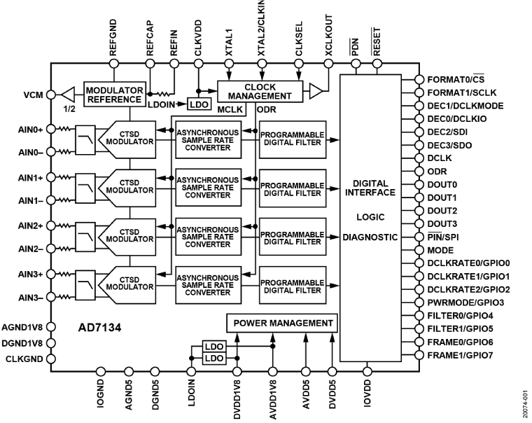
AD7134 Evaluation Board
Analog Devices Inc.
AD7134 Evaluation Board
Analog Devices Inc.
The EVAL-AD7134FMCZ evaluation kit features the AD7134 24-bit, 4-channel, simultaneous sampling, 1.5 MSPS precision alias free analog-to-digital converter (ADC). Two on-board AD7134 ADCs are included to demonstrate multidevice simultaneous sampling. The EVAL-AD7134FMCZ draws power from the system demonstration platform (SDP) EVAL-SDP-CH1Z (SDP-H1) board, and the on-board dc-to-dc regulators regulate an external supply of 8 V to 14 V down to 5 V, 1.8 V, and 1.2 V to supply the AD7134 and peripheral components. Both on-board ADCs have a separate reference of 4.096 V generated by the on-board ADR444. The ADCs have three clock input options and can be clocked by a crystal input, a microelectromechanical system (MEMS) oscillator, or a complementary metal-oxide semiconductor (CMOS) clock. The EVAL-AD7134FMCZ connects to the PC USB port via the SDP-H1 board. The AD7134 evaluation software running on a PC provides full accessibility to the AD7134 device register map, as well as a data analysis interface to display key parameters and graphics from the conversion result in both time and frequency domains. For full details on the AD7134, see the AD7134 data sheet, which must be consulted in conjunction with this user guide when using the EVAL-AD7134FMCZ.
Pack-Side Impedance Track Fuel Gauge

Texas Instruments
Pack-Side Impedance Track Fuel Gauge
Texas Instruments
The Texas Instruments bq27411-G1 reference design is an easy to configure fuel gauging solution for single series cell Li-Ion battery packs. The device requires minimal configuration and uses One Time Programmable (OTP) Non-Volatile Memory (NVM) to avoid an initialization download by the system processor.The bq27411-G1 uses the patented Impedance Track™ algorithm for fuel gauging: and provides information such as remaining battery capacity (mAh): state-of-charge (%): and battery voltage (mV).

ADV3227-EVALZ

Analog Devices Inc.
ADV3227-EVALZ
Analog Devices Inc.
The ADV3226/ADV3227 are high speed 16 ? 16 analog crosspoint switch matrices. They offer a ?3 dB signal bandwidth greater than 750 MHz and channel switch times of less than 20 ns with 1% settling.The ADV3226/ADV3227 include 16 independent output buffers that can be placed into a high impedance state for paralleling crosspoint outputs to prevent off channels from loading the output bus. The ADV3226 has a gain of +1 and the ADV3227 has a gain of +2. They both operate on voltage supplies of ?5 V while consuming only 118 mA (ADV3226) and 133 mA (ADV3227) of idle current. Channel switching is performed via a serial digital control that can accommodate daisy chaining of several devices or via a parallel control to allow updating of an individual output without reprogramming the entire array.The ADV3226/ADV3227 are available in the 100-lead LFCSP package over the extended industrial temperature range of ?40?C to +85?C.Applications Routing of high speed signals including ? ? Video (NTSC, PAL, S, SECAM, YUV, RGB) ? ? Compressed video (MPEG, wavelet) ? ? 3-level digital video (HDB3) Data communications Telecommunications
EVAL-AD1939AZ

Analog Devices Inc.
EVAL-AD1939AZ
Analog Devices Inc.
The AD1939 is a high performance, single-chip codec that provides four analog-to-digital converters (ADCs) with differential input, and eight digital-to-analog converters (DACs) with differential output using the Analog Devices, Inc. patented multibit sigma-delta (?-?) architecture. An SPI port is included, allowing a microcontroller to adjust volume and many other parameters. The AD1939 operates from 3.3 V digital and analog supplies. The AD1939 is available in a 64-lead (differential output) LQFP package.The AD1939 is designed for low EMI. This consideration is apparent in both the system and circuit design architectures. By using the on-board PLL to derive the master clock from the LR clock or from an external crystal, the AD1939 eliminates the need for a separate high frequency master clock and can also be used with a suppressed bit clock. The DACs and ADCs are designed using the latest Analog Devices continuous time architectures to further minimize EMI. By using 3.3 V supplies, power consumption is minimized, further reducing emissions.APPLICATIONS Automotive audio systems Home Theater Systems Set-top boxes Digital audio effects processors


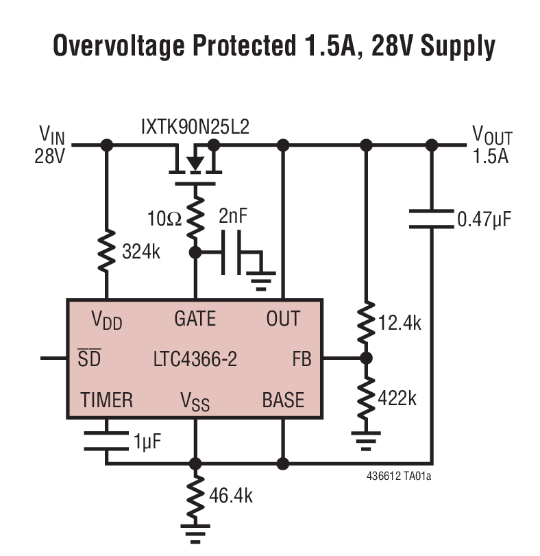
LTC4012CUF Demo Board | Multi-Chemistry 8A Buck Battery Charger with PowerPath Control

Analog Devices Inc.
LTC4012CUF Demo Board | Multi-Chemistry 8A Buck Battery Charger with PowerPath Control
Analog Devices Inc.
Demonstration circuit 1614 features the LTC4012CUF, a multi-chemistry single battery charger controller with PowerPath™ control. The input supply voltage is 13.5V to 20V and is initially configured for a current limit of 10A. The charger float voltage is programmed by jumpers to support 1- to 4- series cells of both Li-Ion/Polymer and Li-iron phosphate (LiFePO4) at 4.2V/cell and 3.6V/cell, for a total of eight settings. The demo board is initially configured for constant-voltage charging of a 12.6V Li-Ion/ Polymer battery and constant-current charging at 8A, though current derating may be necessary due to certain operating conditions.
Improving the Performance of Traditional Flyback-Topology With Two-Switch ?Appro

Texas Instruments
Improving the Performance of Traditional Flyback-Topology With Two-Switch ?Appro
Texas Instruments
This application note explains the basic operation of the two-switch Flyback-power stage, and clarifies benefits and design restrictions not present in traditional Flyback-topology. Power st
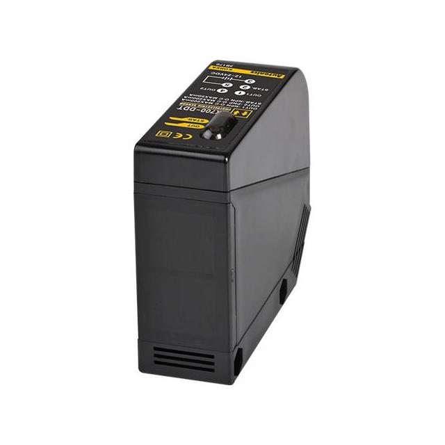
ADP2140CPZ-REDYKIT

Analog Devices Inc.
ADP2140CPZ-REDYKIT
Analog Devices Inc.
The ADP2140 includes a high efficiency, low quiescent 600 mAstepdown dc-to-dc converter and a 300 mA LDO packaged in asmall 10-lead 3 mm ? 3 mm LFCSP. The total solution requiresonly four tiny external components.The buck regulator uses a proprietary high speed current-mode,constant frequency, pulse-width modulation (PWM) controlscheme for excellent stability and transient response. To ensurethe longest battery life in portable applications, the ADP2140 hasa power saving variable frequency mode to reduce switching frequencyunder light loads.The LDO is a low quiescent current, low dropout linear regulatordesigned to operate in a split supply mode with VIN2 as low as1.65 V. The low input voltage minimum allows the LDO to bepowered from the output of the buck regulator increasing efficiencyand reducing power dissipation. The ADP2140 runs frominput voltages of 2.3 V to 5.5 V allowing single Li+/Li? polymer cell, multiple alkaline/NiMH cell, PCMCIA, and other standardpower sources.ADP2140 includes a power-good pin, soft start, and internal?compensation. Numerous power sequencing options are user-selectable through two enable inputs. In autosequencing mode, the highest voltage output enables on the rising edge of EN1.?During logic controlled shutdown, the input disconnects from the output and draws less than 300 nA from the input source.?Other key features include: undervoltage lockout to prevent deep?battery discharge, soft start to prevent input current overshoot?at startup, and both short-circuit protection and thermal overload protection circuits to prevent damage in adverse conditions.When the ADP2140 is used with two 0603 capacitors, one 0402capacitor, one 0402 resistor, and one 0805 chip inductor, the totalsolution size is approximately 90 mm2 resulting in the smallest footprintsolution to meet a variety of portable applications.Applications Mobile phones Personal media players Digital camera and audio devices Portable and battery-powered equipment