OP120
Part Number : OP120
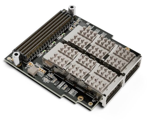
Opsero2X QSFP28 FMC
OP120 Dual QSFP28 FMC for 100G Networking on FPGA Development Boards
Opsero OP120 FMC adds two QSFP28 slots to FPGA carrier boards, delivering up to 200 Gbps of aggregate bandwidth with SyncE support
Opsero OP120 is an FPGA mezzanine card that adds two QSFP28 module slots to FPGA and SoC-based development boards. Each slot accepts QSFP, QSFP+, or QSFP28 optical or copper modules and provides four serial lanes of up to 25 Gbps per lane — an aggregate of 100 Gbps per port and 200 Gbps across both ports. This gives engineers working on 100G Ethernet, Interlaken, CPRI, and other high-speed serial protocols a compact and carrier-agnostic way to prototype and validate their designs.
The card connects to the carrier via a high pin count FMC connector conforming to the VITA 57.1 standard, routing all eight high-speed lanes to the carrier FPGA's gigabit transceivers. An on-board jitter-attenuating clock multiplier supports recovered clock operation and Synchronous Ethernet (SyncE), making the OP120 suitable for timing-sensitive network designs as well as pure throughput workloads. Reference clocks can be sourced from the FPGA, from a recovered data stream, or from an on-board oscillator.
Level translators on the low-speed control signals allow the card to operate with FPGA I/O voltages from 1.2 V to 3.3 V, and test points are provided on key signals to simplify bring-up and debugging. The OP120 ships with example designs and full sources for multiple development boards, including both standalone and PetaLinux builds. These reference designs cover multi-gigabit Ethernet bring-up and give engineers a working starting point, reducing the effort required to go from an FMC installation to a validated data plane.
Features:
Two QSFP28 module slots compatible with QSFP, QSFP+, and QSFP28 modules
Four lanes per port at up to 25 Gbps (100 Gbps per port, 200 Gbps aggregate)
Jitter-attenuating clock multiplier with recovered clock support
Synchronous Ethernet (SyncE) capable clock architecture
Adjustable VADJ range from 1.2 V to 3.3 V with level translators
High pin count FMC connector conforming to VITA 57.1
Test points on key signals for debugging and bring-up
Standalone and PetaLinux example designs with full sources
Support for multiple FPGA development boards out of the box
Supplied with mounting hardware
Applications:
100G Ethernet development and prototyping
10G, 25G, and 40G Ethernet bring-up
Synchronous Ethernet and timing-critical network designs
FPGA-to-FPGA or FPGA-to-switch high-speed interconnects
Data center and telecom infrastructure prototyping
5G fronthaul and backhaul development
High-throughput data acquisition and streaming
Network test and measurement equipment
Interlaken and CPRI protocol development
Optical module evaluation and qualification
OP120
Part Number : OP120
Opsero2X QSFP28 FMC
OP120 Dual QSFP28 FMC for 100G Networking on FPGA Development Boards
Opsero OP120 FMC adds two QSFP28 slots to FPGA carrier boards, delivering up to 200 Gbps of aggregate bandwidth with SyncE support
Opsero OP120 is an FPGA mezzanine card that adds two QSFP28 module slots to FPGA and SoC-based development boards. Each slot accepts QSFP, QSFP+, or QSFP28 optical or copper modules and provides four serial lanes of up to 25 Gbps per lane — an aggregate of 100 Gbps per port and 200 Gbps across both ports. This gives engineers working on 100G Ethernet, Interlaken, CPRI, and other high-speed serial protocols a compact and carrier-agnostic way to prototype and validate their designs.
The card connects to the carrier via a high pin count FMC connector conforming to the VITA 57.1 standard, routing all eight high-speed lanes to the carrier FPGA's gigabit transceivers. An on-board jitter-attenuating clock multiplier supports recovered clock operation and Synchronous Ethernet (SyncE), making the OP120 suitable for timing-sensitive network designs as well as pure throughput workloads. Reference clocks can be sourced from the FPGA, from a recovered data stream, or from an on-board oscillator.
Level translators on the low-speed control signals allow the card to operate with FPGA I/O voltages from 1.2 V to 3.3 V, and test points are provided on key signals to simplify bring-up and debugging. The OP120 ships with example designs and full sources for multiple development boards, including both standalone and PetaLinux builds. These reference designs cover multi-gigabit Ethernet bring-up and give engineers a working starting point, reducing the effort required to go from an FMC installation to a validated data plane.
Features:
Two QSFP28 module slots compatible with QSFP, QSFP+, and QSFP28 modules
Four lanes per port at up to 25 Gbps (100 Gbps per port, 200 Gbps aggregate)
Jitter-attenuating clock multiplier with recovered clock support
Synchronous Ethernet (SyncE) capable clock architecture
Adjustable VADJ range from 1.2 V to 3.3 V with level translators
High pin count FMC connector conforming to VITA 57.1
Test points on key signals for debugging and bring-up
Standalone and PetaLinux example designs with full sources
Support for multiple FPGA development boards out of the box
Supplied with mounting hardware
Applications:
100G Ethernet development and prototyping
10G, 25G, and 40G Ethernet bring-up
Synchronous Ethernet and timing-critical network designs
FPGA-to-FPGA or FPGA-to-switch high-speed interconnects
Data center and telecom infrastructure prototyping
5G fronthaul and backhaul development
High-throughput data acquisition and streaming
Network test and measurement equipment
Interlaken and CPRI protocol development
Optical module evaluation and qualification


