MAX414BESD+
Part Number : MAX414BESD+
Analog Devices Inc.Precision Amplifiers Quad 28MHz Low-V Low-Noise Precision
LTM4682EY#PBF
Part Number : LTM4682EY#PBF
Analog Devices Inc.Dc-Dc Converter, 0.7 To 1.35V, 31.25A Rohs Compliant: Yes |Analog Devices LTM4682EY#PBF
LTM4702IY
Part Number : LTM4702IY
Analog Devices Inc.18 Vin, 8A Silent Switcher Umodule Reg |Analog Devices LTM4702IY
LT3514HFE#PBF
Part Number : LT3514HFE#PBF
Analog Devices Inc.Sw Regltr, 3.2-36V, 2.1Mhz, Tssop-Ep-24 Rohs Compliant: Yes |Analog Devices LT3514HFE#PBF

LTM8048MPY
Part Number : LTM8048MPY
Analog Devices Inc.Isolated Module DC DC Converter 2 Output 2.5 ~ 13V 1.2 ~ 12V 440mA, 300mA 3.1V - 32V Input

LTC4367HMS8-1
Part Number : LTC4367HMS8-1
Analog Devices Inc.Overvoltage, Undervoltage Protection PMIC 8-MSOP

MAX1636EAP
Part Number : MAX1636EAP
Analog Devices Inc.Buck Regulator Positive Output Step-Down DC-DC Controller IC 20-SSOP
MAX6386XS16D3+T
Part Number : MAX6386XS16D3+T
Analog Devices Inc.Supervisory Circuits SC70/ DFN, Single/Dual Low-Voltage, Low-Power P Reset Circuits
MAX6386XS16D3-T
Part Number : MAX6386XS16D3-T
Analog Devices Inc.Supervisor Open Drain or Open Collector 1 Channel SC-70-4
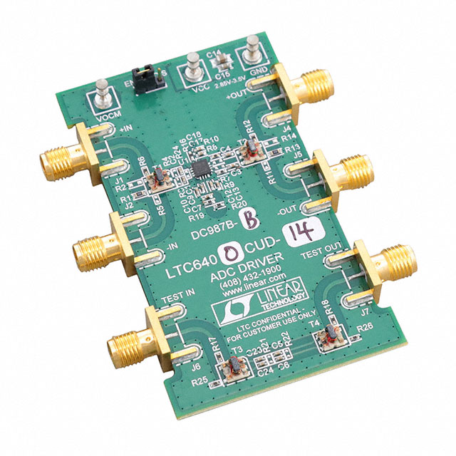
LTC6400-14
Part Number : LTC6400-14
Analog Devices Inc.LTC6400-14 1 - Single Channels per IC Differential Amplifier Evaluation Board


78M6610 LMU/BAP
Part Number : 78M6610 LMU/BAP
Analog Devices Inc.Single Phase Meter IC 24-TQFN (4x4)
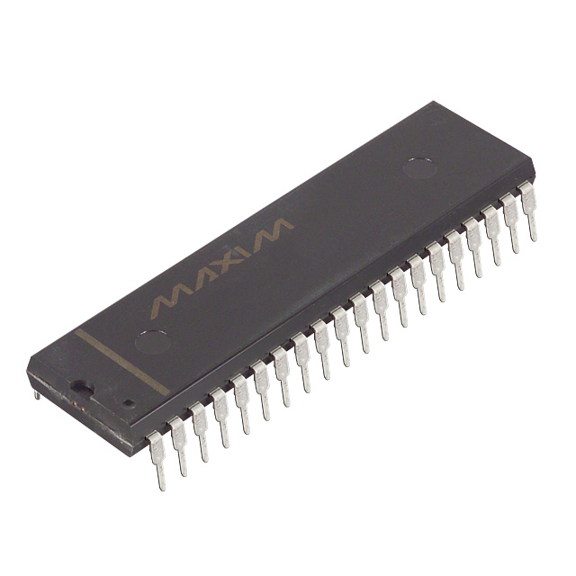
DS80C320-MNG
Part Number : DS80C320-MNG
Analog Devices Inc.8051 80C Microcontroller IC 8-Bit 25MHz ROMless 40-PDIP

LTC2424CG
Part Number : LTC2424CG
Analog Devices Inc.20 Bit Analog to Digital Converter 4 Input 1 Sigma-Delta 28-SSOP
ICM7556IPD+
Part Number : ICM7556IPD+
Analog Devices Inc.Timers & Support Products Low-Power, General-Purpose Timer

LT8607IMSE
Part Number : LT8607IMSE
Analog Devices Inc.Buck Switching Regulator IC Positive Adjustable 1.8V 1 Output 750mA 10-TFSOP, 10-MSOP (0.118", 3.00mm Width) Exposed Pad

LTM4643MPY
Part Number : LTM4643MPY
Analog Devices Inc.Non-Isolated PoL Module DC DC Converter 4 Output 0.6 ~ 3.3V 0.6 ~ 3.3V 0.6 ~ 3.3V 3A, 3A, 3A, 3A 4V - 20V Input


