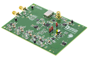
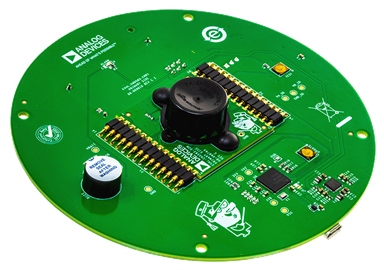
DC1930A
Part Number : DC1930A
Analog Devices Inc.High Current Synchronous Step-Down LED Driver Features:Ideal for Driving Up to 40A LEDsUp to 3000:1 PWM Dimming20:1 Analog Dimming±3% Current Regulation Accuracy±3% Voltage Regulation AccuracyUnique Inverting Buck-Boost Topology Allows Grounded Heat Sink to Be Used for RGB LEDs3.3V to 36V Input Voltage RangePeak Current Mode with DC LED Current SensingOpen and Shorted LED Protection and Fault ReportingFloating LED Driver Allows Single Power Solution to Drive Multicolor LEDs or Single LED with Three Different Regulated CurrentsThermally Enhanced 5mm × 6mm QFN 36-Lead Package

ADA4097-1BUJZ-R5
Part Number : ADA4097-1BUJZ-R5
Analog Devices Inc.50 V, 130 kHz, 32.5 A, Robust, Over-The-Top Precision Op Amp Features: Ultrawide common-mode input range: −VS − 0.1 V to −VS + 70 V Wide power supply voltage range: +3 V to +50 V (to ±25 V for PSRR) Low power supply current: 32.5 μA (typical) Low input offset voltage: ±60 μV maximum Low input offset voltage drift: ±1 μV/°C maximum (B grade) Low input voltage noise 6 Hz typical 1/f noise corner 1000 nV p-p typical at 0.1 Hz to 10 Hz GBP: 130 kHz typical for fTEST = 250 Hz Slew rate: 0.1 V/μs typical at ΔVOUT = 4 V Low power supply current shutdown: 20 μA maximum Low input offset current: ±300 pA maximum Large signal voltage gain: 120 dB minimum for ΔVOUT = 3.5 V CMRR: 120 dB minimum at VCM = −0.1 V to +70 V PSRR: 123 dB minimum at VSY = +3 V to ±25 V Input overdrive tolerant with no phase reversal ±2 kV HBM and ±1.25 kV FICDM Wide temperature range: −55°C to +150°C (H grade) Shutdown feature available for single 6-lead TSOT and dual 10-lead LFCSP packages

ADA4097-2HCPZ
Part Number : ADA4097-2HCPZ
Analog Devices Inc.50 V, 130 kHz, 32.5 A per Channel, Robust, Over-The-Top, Precision Op Amp Features: Ultrawide common-mode input range: −VS − 0.1 V to −VS + 70 V Wide power supply voltage range: +3 V to +50 V (to ±25 V for PSRR) Low power supply current: 32.5 μA (typical) Low input offset voltage: ±60 μV maximum Low input offset voltage drift: ±1 μV/°C maximum (B grade) Low input voltage noise 6 Hz typical 1/f noise corner 1000 nV p-p typical at 0.1 Hz to 10 Hz GBP: 130 kHz typical for fTEST = 250 Hz Slew rate: 0.1 V/μs typical at ΔVOUT = 4 V Low power supply current shutdown: 20 μA maximum Low input offset current: ±300 pA maximum Large signal voltage gain: 120 dB minimum for ΔVOUT = 3.5 V CMRR: 120 dB minimum at VCM = −0.1 V to +70 V PSRR: 123 dB minimum at VSY = +3 V to ±25 V Input overdrive tolerant with no phase reversal ±2 kV HBM and ±1.25 kV FICDM Wide temperature range: −55°C to +150°C (H grade) Shutdown feature available for single 6-lead TSOT and dual 10-lead LFCSP packages
ADA4097-2HRZ
Part Number : ADA4097-2HRZ
Analog Devices Inc.50 V, 130 kHz, 32.5 A per Channel, Robust, Over-The-Top, Precision Op Amp Features: Ultrawide common-mode input range: −VS − 0.1 V to −VS + 70 V Wide power supply voltage range: +3 V to +50 V (to ±25 V for PSRR) Low power supply current: 32.5 μA (typical) Low input offset voltage: ±60 μV maximum Low input offset voltage drift: ±1 μV/°C maximum (B grade) Low input voltage noise 6 Hz typical 1/f noise corner 1000 nV p-p typical at 0.1 Hz to 10 Hz GBP: 130 kHz typical for fTEST = 250 Hz Slew rate: 0.1 V/μs typical at ΔVOUT = 4 V Low power supply current shutdown: 20 μA maximum Low input offset current: ±300 pA maximum Large signal voltage gain: 120 dB minimum for ΔVOUT = 3.5 V CMRR: 120 dB minimum at VCM = −0.1 V to +70 V PSRR: 123 dB minimum at VSY = +3 V to ±25 V Input overdrive tolerant with no phase reversal ±2 kV HBM and ±1.25 kV FICDM Wide temperature range: −55°C to +150°C (H grade) Shutdown feature available for single 6-lead TSOT and dual 10-lead LFCSP packages
ADA4097-2HRZ-RL7
Part Number : ADA4097-2HRZ-RL7
Analog Devices Inc.50 V, 130 kHz, 32.5 A per Channel, Robust, Over-The-Top, Precision Op Amp Features: Ultrawide common-mode input range: −VS − 0.1 V to −VS + 70 V Wide power supply voltage range: +3 V to +50 V (to ±25 V for PSRR) Low power supply current: 32.5 μA (typical) Low input offset voltage: ±60 μV maximum Low input offset voltage drift: ±1 μV/°C maximum (B grade) Low input voltage noise 6 Hz typical 1/f noise corner 1000 nV p-p typical at 0.1 Hz to 10 Hz GBP: 130 kHz typical for fTEST = 250 Hz Slew rate: 0.1 V/μs typical at ΔVOUT = 4 V Low power supply current shutdown: 20 μA maximum Low input offset current: ±300 pA maximum Large signal voltage gain: 120 dB minimum for ΔVOUT = 3.5 V CMRR: 120 dB minimum at VCM = −0.1 V to +70 V PSRR: 123 dB minimum at VSY = +3 V to ±25 V Input overdrive tolerant with no phase reversal ±2 kV HBM and ±1.25 kV FICDM Wide temperature range: −55°C to +150°C (H grade) Shutdown feature available for single 6-lead TSOT and dual 10-lead LFCSP packages

ADA4098-2BCPZ-RL7
Part Number : ADA4098-2BCPZ-RL7
Analog Devices Inc.50 V, 1 MHz, 165 A per Channel, Robust, Over-The-Top, Precision Op Amps Features: Ultrawide common-mode input range: −VS − 0.1 V to −VS + 70 V Wide power supply voltage range: +3 V to +50 V (to ±25 V for PSRR) Low power supply current: 165 μA per channel (typical) Low input offset voltage: ±35 μV maximum Low input offset voltage drift: ±0.5 μV/°C maximum (B grade) Low input voltage noise 1/f noise corner: 6 Hz typical 400 nV p-p typical at 0.1 Hz to 10 Hz 17 nV/√Hz typical at 100 Hz High speed GBP: 1.05 MHz typical for fTEST = 2.5 kHz Slew rate: 0.85 V/μs typical at ΔVOUT = 25 V Low power supply current shutdown: 20 μA maximum Low input offset current: ±700 pA maximum Large signal voltage gain: 126 dB minimum for ΔVOUT = 3.5 V CMRR: 120 dB minimum at VCM = −0.1 V to +70 V PSRR: 123 dB minimum at VSY = +3 V to ±25 V Input overdrive tolerant with no phase reversal ±3 kV HBM and ±1.25 kV FICDM Wide temperature range: −55°C to +150°C (H grade)
ADA4098-2BRZ
Part Number : ADA4098-2BRZ
Analog Devices Inc.50 V, 1 MHz, 165 A per Channel, Robust, Over-The-Top, Precision Op Amps Features: Ultrawide common-mode input range: −VS − 0.1 V to −VS + 70 V Wide power supply voltage range: +3 V to +50 V (to ±25 V for PSRR) Low power supply current: 165 μA per channel (typical) Low input offset voltage: ±35 μV maximum Low input offset voltage drift: ±0.5 μV/°C maximum (B grade) Low input voltage noise 1/f noise corner: 6 Hz typical 400 nV p-p typical at 0.1 Hz to 10 Hz 17 nV/√Hz typical at 100 Hz High speed GBP: 1.05 MHz typical for fTEST = 2.5 kHz Slew rate: 0.85 V/μs typical at ΔVOUT = 25 V Low power supply current shutdown: 20 μA maximum Low input offset current: ±700 pA maximum Large signal voltage gain: 126 dB minimum for ΔVOUT = 3.5 V CMRR: 120 dB minimum at VCM = −0.1 V to +70 V PSRR: 123 dB minimum at VSY = +3 V to ±25 V Input overdrive tolerant with no phase reversal ±3 kV HBM and ±1.25 kV FICDM Wide temperature range: −55°C to +150°C (H grade)
ADA4098-2BRZ-RL7
Part Number : ADA4098-2BRZ-RL7
Analog Devices Inc.50 V, 1 MHz, 165 A per Channel, Robust, Over-The-Top, Precision Op Amps Features: Ultrawide common-mode input range: −VS − 0.1 V to −VS + 70 V Wide power supply voltage range: +3 V to +50 V (to ±25 V for PSRR) Low power supply current: 165 μA per channel (typical) Low input offset voltage: ±35 μV maximum Low input offset voltage drift: ±0.5 μV/°C maximum (B grade) Low input voltage noise 1/f noise corner: 6 Hz typical 400 nV p-p typical at 0.1 Hz to 10 Hz 17 nV/√Hz typical at 100 Hz High speed GBP: 1.05 MHz typical for fTEST = 2.5 kHz Slew rate: 0.85 V/μs typical at ΔVOUT = 25 V Low power supply current shutdown: 20 μA maximum Low input offset current: ±700 pA maximum Large signal voltage gain: 126 dB minimum for ΔVOUT = 3.5 V CMRR: 120 dB minimum at VCM = −0.1 V to +70 V PSRR: 123 dB minimum at VSY = +3 V to ±25 V Input overdrive tolerant with no phase reversal ±3 kV HBM and ±1.25 kV FICDM Wide temperature range: −55°C to +150°C (H grade)
ADA4098-2HCPZ-RL7
Part Number : ADA4098-2HCPZ-RL7
Analog Devices Inc.50 V, 1 MHz, 165 A per Channel, Robust, Over-The-Top, Precision Op Amps Features: Ultrawide common-mode input range: −VS − 0.1 V to −VS + 70 V Wide power supply voltage range: +3 V to +50 V (to ±25 V for PSRR) Low power supply current: 165 μA per channel (typical) Low input offset voltage: ±35 μV maximum Low input offset voltage drift: ±0.5 μV/°C maximum (B grade) Low input voltage noise 1/f noise corner: 6 Hz typical 400 nV p-p typical at 0.1 Hz to 10 Hz 17 nV/√Hz typical at 100 Hz High speed GBP: 1.05 MHz typical for fTEST = 2.5 kHz Slew rate: 0.85 V/μs typical at ΔVOUT = 25 V Low power supply current shutdown: 20 μA maximum Low input offset current: ±700 pA maximum Large signal voltage gain: 126 dB minimum for ΔVOUT = 3.5 V CMRR: 120 dB minimum at VCM = −0.1 V to +70 V PSRR: 123 dB minimum at VSY = +3 V to ±25 V Input overdrive tolerant with no phase reversal ±3 kV HBM and ±1.25 kV FICDM Wide temperature range: −55°C to +150°C (H grade)

ADA4099-1BUJZ-R5
Part Number : ADA4099-1BUJZ-R5
Analog Devices Inc.50 V, 8 MHz, 1.5 mA per Channel, Robust, Over-The-Top, Precision Op Amps Features: Ultrawide common-mode range: −VS − 0.1 V to −VS + 70 V Wide power supply voltage range: (VSY): +3.15 V to +50 V (±25 V for PSRR) Low supply current: 1.5 mA per channel (typical) Low input offset voltage: ±40 μV maximum Low input offset voltage drift: ±0.4 μV/°C maximum Low voltage noise: 1/f noise corner: 6 Hz typical 150 nV p-p typical at 0.1 Hz to 10 Hz 7 nV/√Hz typical at 100 Hz (en) High speed GBP: 8 MHz typical Slew rate: 5.5 V/μs typical at ΔVOUT = 25 V Low power shutdown: 20 μA maximum Low input bias current: ±10 nA maximum Large signal voltage gain: 120 dB minimum CMRR: 118 dB, minimum PSRR: 123 dB, minimum Input overdrive tolerant with no phase reversal ±2 kV HBM and ±1.25 kV FICDM Wide temperature range: −55°C to +150°C (H grade)
ADA4099-1HUJZ-RL7
Part Number : ADA4099-1HUJZ-RL7
Analog Devices Inc.50 V, 8 MHz, 1.5 mA per Channel, Robust, Over-The-Top, Precision Op Amps Features: Ultrawide common-mode range: −VS − 0.1 V to −VS + 70 V Wide power supply voltage range: (VSY): +3.15 V to +50 V (±25 V for PSRR) Low supply current: 1.5 mA per channel (typical) Low input offset voltage: ±40 μV maximum Low input offset voltage drift: ±0.4 μV/°C maximum Low voltage noise: 1/f noise corner: 6 Hz typical 150 nV p-p typical at 0.1 Hz to 10 Hz 7 nV/√Hz typical at 100 Hz (en) High speed GBP: 8 MHz typical Slew rate: 5.5 V/μs typical at ΔVOUT = 25 V Low power shutdown: 20 μA maximum Low input bias current: ±10 nA maximum Large signal voltage gain: 120 dB minimum CMRR: 118 dB, minimum PSRR: 123 dB, minimum Input overdrive tolerant with no phase reversal ±2 kV HBM and ±1.25 kV FICDM Wide temperature range: −55°C to +150°C (H grade)
ADA4099-2BRMZ-RL7
Part Number : ADA4099-2BRMZ-RL7
Analog Devices Inc.50 V, 8 MHz, 1.5 mA per Channel, Robust, Over-The-Top, Precision Op Amps Features: Ultrawide common-mode range: −VS − 0.1 V to −VS + 70 V Wide power supply voltage range: (VSY): +3.15 V to +50 V (±25 V for PSRR) Low supply current: 1.5 mA per channel (typical) Low input offset voltage: ±40 μV maximum Low input offset voltage drift: ±0.4 μV/°C maximum Low voltage noise: 1/f noise corner: 6 Hz typical 150 nV p-p typical at 0.1 Hz to 10 Hz 7 nV/√Hz typical at 100 Hz (en) High speed GBP: 8 MHz typical Slew rate: 5.5 V/μs typical at ΔVOUT = 25 V Low power shutdown: 20 μA maximum Low input bias current: ±10 nA maximum Large signal voltage gain: 120 dB minimum CMRR: 118 dB, minimum PSRR: 123 dB, minimum Input overdrive tolerant with no phase reversal ±2 kV HBM and ±1.25 kV FICDM Wide temperature range: −55°C to +150°C (H grade)
ADA4099-2HCPZ
Part Number : ADA4099-2HCPZ
Analog Devices Inc.50 V, 8 MHz, 1.5 mA per Channel, Robust, Over-The-Top, Precision Op Amps Features: Ultrawide common-mode range: −VS − 0.1 V to −VS + 70 V Wide power supply voltage range: (VSY): +3.15 V to +50 V (±25 V for PSRR) Low supply current: 1.5 mA per channel (typical) Low input offset voltage: ±40 μV maximum Low input offset voltage drift: ±0.4 μV/°C maximum Low voltage noise: 1/f noise corner: 6 Hz typical 150 nV p-p typical at 0.1 Hz to 10 Hz 7 nV/√Hz typical at 100 Hz (en) High speed GBP: 8 MHz typical Slew rate: 5.5 V/μs typical at ΔVOUT = 25 V Low power shutdown: 20 μA maximum Low input bias current: ±10 nA maximum Large signal voltage gain: 120 dB minimum CMRR: 118 dB, minimum PSRR: 123 dB, minimum Input overdrive tolerant with no phase reversal ±2 kV HBM and ±1.25 kV FICDM Wide temperature range: −55°C to +150°C (H grade)

ADA4177-1ARMZ-RL
Part Number : ADA4177-1ARMZ-RL
Analog Devices Inc.OVP and EMI Protected, Precision, Low Noise and Bias Current Single Op Amp Features: Low offset voltage: 60 μV maximum at 25°C (8-lead and 14-lead SOIC) Low offset voltage drift: 1 μV/°C maximum (8-lead and 14-lead SOIC) Low input bias current: 1 nA maximum at 25°C Low voltage noise density: 8 nV/√Hz typical at 1 kHz Large signal voltage gain (AVO): 100 dB minimum over full supply voltage and operating temperature Input overvoltage protection to 32 V above and below the supply voltage rail Integrated EMI filter 70 dB typical rejection at 1000 MHz 90 dB typical rejection at 2400 MHz Rail-to-rail output swing Low supply current: 500 μA typical per amplifier Wide bandwidth Gain bandwidth product (AV = 100): 3.5 MHz typical Unity-gain crossover (AV = 1): 3.5 MHz typical −3 dB bandwidth (AV = 1): 6 MHz typical Dual-supply operation Specified at ±5 V to ±15 V, operates over ±2.5 V to ±18 V Unity-gain stable No phase reversal Long-term offset voltage drift (10,000 hours): 2 μV typical Temperature hysteresis: 2 μV typical

ADA4254ACPZ
Part Number : ADA4254ACPZ
Analog Devices Inc.Zero Drift, High Voltage, Low Power, Programmable Gain Instrumentation Amplifier Features: Optimized for ADC synchronization Low power: 22 mW (±12 V supplies) 12 binary gain steps from 1/16 V/V to 128 V/V 3 scaling gains: 1 V/V, 1.25 V/V, and 1.375 V/V ±60 V protected input multiplexer Excellent dc precision Low input offset voltage: ±14 μV maximum Low input offset voltage drift: ±0.08 μV/°C maximum Gain calibration via ROM Low gain drift: ±1 ppm/°C maximum High CMRR: 116 dB minimum, G = 1 V/V Low input bias current: ±1.5 nA maximum High input impedance Integrated input EMI filtering Wide input supply range: ±5 V to ±28 V Dedicated output amplifier supplies 7 GPIO ports with special functions Sequential chip select mode External multiplexer control Excitation current sources SPI port with checksum (CRC) support Internal fault detection Wire break test currents On-chip test multiplexer 28-lead, 5 mm × 5 mm LFCSP, 24-lead TSSOP Specified temperature range: −40°C to +105°C
ADA4254ARUZ-RL
Part Number : ADA4254ARUZ-RL
Analog Devices Inc.Zero Drift, High Voltage, Low Power, Programmable Gain Instrumentation Amplifier Features: Optimized for ADC synchronization Low power: 22 mW (±12 V supplies) 12 binary gain steps from 1/16 V/V to 128 V/V 3 scaling gains: 1 V/V, 1.25 V/V, and 1.375 V/V ±60 V protected input multiplexer Excellent dc precision Low input offset voltage: ±14 μV maximum Low input offset voltage drift: ±0.08 μV/°C maximum Gain calibration via ROM Low gain drift: ±1 ppm/°C maximum High CMRR: 116 dB minimum, G = 1 V/V Low input bias current: ±1.5 nA maximum High input impedance Integrated input EMI filtering Wide input supply range: ±5 V to ±28 V Dedicated output amplifier supplies 7 GPIO ports with special functions Sequential chip select mode External multiplexer control Excitation current sources SPI port with checksum (CRC) support Internal fault detection Wire break test currents On-chip test multiplexer 28-lead, 5 mm × 5 mm LFCSP, 24-lead TSSOP Specified temperature range: −40°C to +105°C
ADA4254CP-EBZ
Part Number : ADA4254CP-EBZ
Analog Devices Inc.Zero Drift, High Voltage, Low Power, Programmable Gain Instrumentation Amplifier Features: Optimized for ADC synchronization Low power: 22 mW (±12 V supplies) 12 binary gain steps from 1/16 V/V to 128 V/V 3 scaling gains: 1 V/V, 1.25 V/V, and 1.375 V/V ±60 V protected input multiplexer Excellent dc precision Low input offset voltage: ±14 μV maximum Low input offset voltage drift: ±0.08 μV/°C maximum Gain calibration via ROM Low gain drift: ±1 ppm/°C maximum High CMRR: 116 dB minimum, G = 1 V/V Low input bias current: ±1.5 nA maximum High input impedance Integrated input EMI filtering Wide input supply range: ±5 V to ±28 V Dedicated output amplifier supplies 7 GPIO ports with special functions Sequential chip select mode External multiplexer control Excitation current sources SPI port with checksum (CRC) support Internal fault detection Wire break test currents On-chip test multiplexer 28-lead, 5 mm × 5 mm LFCSP, 24-lead TSSOP Specified temperature range: −40°C to +105°C
ADA4254RU-EBZ
Part Number : ADA4254RU-EBZ
Analog Devices Inc.Zero Drift, High Voltage, Low Power, Programmable Gain Instrumentation Amplifier Features: Optimized for ADC synchronization Low power: 22 mW (±12 V supplies) 12 binary gain steps from 1/16 V/V to 128 V/V 3 scaling gains: 1 V/V, 1.25 V/V, and 1.375 V/V ±60 V protected input multiplexer Excellent dc precision Low input offset voltage: ±14 μV maximum Low input offset voltage drift: ±0.08 μV/°C maximum Gain calibration via ROM Low gain drift: ±1 ppm/°C maximum High CMRR: 116 dB minimum, G = 1 V/V Low input bias current: ±1.5 nA maximum High input impedance Integrated input EMI filtering Wide input supply range: ±5 V to ±28 V Dedicated output amplifier supplies 7 GPIO ports with special functions Sequential chip select mode External multiplexer control Excitation current sources SPI port with checksum (CRC) support Internal fault detection Wire break test currents On-chip test multiplexer 28-lead, 5 mm × 5 mm LFCSP, 24-lead TSSOP Specified temperature range: −40°C to +105°C

ADA4255ACPZ-R7
Part Number : ADA4255ACPZ-R7
Analog Devices Inc.Zero Drift, High Voltage, Programmable Gain Instrumentation Amplifier with Charge Pump Features:Integrated bipolar charge pumpSimplified isolation requirements Wide input range on low voltage suppliesDedicated output amplifier supplies for ADC protectionLow power: 83 mW (DVDD = 3 V, VDDCP = 5 V)36 precision gains from 1/16 V/V to 176 V/VRobust ±60 V protected 2:1 input multiplexerLow input bias current: ±1.5 nA maximum at TA = 25°CIntegrated input EMI filtering7 GPIOx ports with special functionsSequential chip select modeExcellent dc precisionLow input offset voltage: ±14 µV maximum Low input offset voltage drift: ±0.08 µV/°C maximum Gain calibration via internal memory Low gain drift: ±1 ppm/°C maximum High CMRR: 111 dB minimum, G = 1 V/VExcitation current sourceSPI port with checksum (CRC) supportInternal/external fault detectionCompact 28-lead, 5 mm × 5 mm LFCSPSpecified temperature range: 40°C to +105°C

ADA4500-2ACPZ-RL
Part Number : ADA4500-2ACPZ-RL
Analog Devices Inc.10 MHz, 14.5 nV/Hz, Rail-to-Rail I/O, Zero Input Crossover Distortion Amplifier Features: Power supply rejection ratio (PSRR): 98 dB minimum Common-mode rejection ratio (CMRR): 95 dB minimum Offset voltage: 120 μV maximum Single-supply operation: 2.7 V to 5.5 V Dual-supply operation: ±1.35 V to ±2.75 V Wide bandwidth: 10 MHz Rail-to-rail input and output Low noise 2 μV p-p from 0.1 Hz to 10 Hz 14.5 nV/√Hz at 1 kHz Very low input bias current: 2 pA maximum