
DC3020A
Analog Devices Inc.The LT8636/LT8637 synchronous step-down regulator features Silent Switcher architecture designed to minimize EMI emissions while delivering high efficiency at high switching frequencies. Peak current mode control with a 30ns minimum on-time allows high step-down ratios even at high switching frequencies.The LT8636?s ultralow 2.5?A quiescent current?with the output in full regulation?enables applications requiring highest efficiency at very small load currents. The LT8637 has external compensation to enable current sharing and fast transient response at high switching frequencies. A CLKOUT pin enables synchronizing other regulators to the LT8636/LT8637.Burst Mode operation enables ultralow standby current consumption, forced continuous mode can control frequency harmonics across the entire output load range, or spread spectrum operation can further reduce EMI emissions. Soft-start and tracking functionality is accessed via the TR/SS pin, and an accurate input voltage UVLO threshold can be set using the EN/UV pin.APPLICATIONS Automotive and Industrial Supplies General Purpose Step-Down

LT4200 | 12V, 50A Hot Swap E-Fuse
Analog Devices Inc.Demonstration circuit 3024A showcases the LT4200 50A hot swap E-fuse with guaranteed SOA. Included on the board are input voltage dividers for undervoltage and overvoltage protection, LEDs to indicate input voltage, output voltage, fault and power bad conditions, and jumpers to enable auto retry and to select circuit breaker delay. Turrets are provided for monitoring input voltage, output voltage, output status, and most of the pins on the LT4200.

LTC3307B | 3.3V to 1.8V at 3A, 6.6MHz Low EMI Buck Regulator in a 0.47cm2 Solution
Analog Devices Inc.Demonstration circuit 3054A-A features the LTC3307B 5V, 3A synchronous step-down Silent Switcher® operating as a 6.6MHz, 3.3V to 1.8V 3A buck regulator. The LTC3307B supports adjustable output voltages from 0.5V to VIN, and operating frequencies from 3MHz up to 10MHz. The LTC3307B is a compact, ultralow emission, high efficiency, and high speed synchronous monolithic step-down switching regulator. A minimum on-time of 22ns enables high VIN to low VOUT conversion ratios at high switching frequencies.
The DC3054A-A operating mode may be selected as Burst Mode® operation, skip or forced continuous (FC) mode. Setting JP1 to the FC/SYNC position will allow the LTC3307B to sync to a clock frequency from 3MHz to 10MHz. The LTC3307B operates in forced continuous mode when syncing to an external clock. The DC3054A-A is set to a fixed 6.6MHz.
The DC3054A-A is set to a fixed 6.6MHz frequency by connecting RT to VIN through a 0Ω resistor, R9. The frequency can be easily changed by removing R9 and setting an appropriate resistor in the R4 location to obtain the desired frequency. Refer to the LTC3307B data sheet for the proper RT value for a desired switching frequency.
The LTC3307B data sheet gives a complete description of the device, operation and application information. The data sheet must be read in conjunction with the demo manual. The LTC3307B is assembled in a 2mm × 2mm LQFN package with exposed pads for low thermal resistance. The layout recommendations for low EMI operation and maximum thermal performance are available in the data sheet section Low EMI PCB Layout.

LT3002 Demo Board | Micropower No-Opto Isolated Flyback Converter with 65V/3.5A Switch
Analog Devices Inc.Demonstration circuit 3077A is a compact no-opto isolated flyback converter featuring the LT3002. The DC3077A outputs 12V and maintains tight regulation with a load current from 5mA up to 1.1A over an input voltage from 10V to 30V. The output current capability increases with the input voltage, as shown in the Performance Summary table.
Transformer leakage inductance causes a voltage spike on the primary side after the power switch turns off. The leakage inductance spike is limited within the MOSFET’s voltage rating of 65V with an RC snubber and a TVS clamp which damp the ringing and clamp the MOSFET drain voltage to a safe level.
The Performance Summary table summarizes the performance of the demo board at room temperature. The DC3077A demo circuit can be easily modified for different applications with some pre-designed transformers.
The LT3002 data sheet gives a complete description of the part, operation and application information. The data sheet must be read in conjunction with this quick start guide for demo circuit 3077A.

LTM4681 | PolyPhase Single Output Step-Down μModule Regulator with Digital PSM: 2 × LTM4681 at 240A
Analog Devices Inc.Demonstration circuit 3082A-A features the LTM4681: the wide input and output voltage range, high efficiency and power density, high current PolyPhase® single output DC/DC step-down μModule® regulator with digital power system management. DC3082A-A is configured as 8-phase single output using 2 × LTM4681. The factory default input voltage is 12V typical, output voltage is 1V at 240A typical or 250A peak with recommended 400LFM forced airflow. The demo board output voltages can be adjusted from 0.6V to 1V. Programming the output voltages to any value that is greater than 1V, requires derating output current based on thermal derating curves provided in the data sheet of the LTM4681. Heat sink or other appropriate electronic cooling systems can also be used in conjunction with forced airflow to further optimize the output power when the output is on and loaded with maximum output current. The factory default switching frequency is preset at 350kHz typical. DC3082A-A comes with PMBus interface and digital power system management functions. An onboard 12-pin connector is available for users to connect the dongle DC1613A to the demo board, provides an easy way to communicate and program the part using LTpowerPlay® software development tool. LTpowerPlay software and I2C/PMBus/SMBus dongle DC1613A allows users to monitor real time telemetry of input and output voltages, input and output current, switching frequency, internal IC die temperatures, power stage component temperatures and fault logs. Programmable parameters include device address, output voltages, control loop compensation, switching frequency, phase interleaving, DCM or CCM Mode of operation, digital soft-start, sequencing, and time based shutdown, fault responses to input and output overvoltage, output overcurrent, IC die and power component overtemperatures.
The LTM4681 is available in a thermally enhanced, low profile 330-Lead (15mm × 22mm × 8.17mm) BGA package. It is recommended to read the data sheet and demo manual of LTM4681 prior to using or making any hardware changes to DC3082A-A.
LTpowerPlay software can be downloaded here.
USB to PMBus Controller Dongle DC1613A for use with LTpowerPlay is available here.

DC309A
Analog Devices Inc.The LTC1773 is a current mode synchronous buck regulator controller that drives external complementary power MOSFETs using a fixed frequency architecture. The operating supply range is from 2.65V to 8.5V, making it suitable for 1- or 2-cell lithium-ion battery powered applications. Burst Mode? operation provides high efficiency at low load currents. 100% duty cycle provides low dropout operation which extends operating time in battery-operated systems.The operating frequency is internally set at 550kHz, allowing the use of small surface mount inductors. For switching-noise sensitive applications, it can be synchronized up to 750kHz. Peak current limit is user programmable with an external high side sense resistor. A SYNC/FCB control pin guarantees regulation of secondary windings regardless of load on the main output by forcing continuous operation. Burst Mode operation is inhibited during synchronization or when the SYNC/FCB pin is pulled low to reduce noise and RF interference. Soft-start is provided by an external capacitor.Synchronous rectification increases efficiency and eliminates the need for a Schottky diode, saving components and board space. The LTC1773 comes in a 10-lead MSOP package.Applications Cellular Telephones RF PA Supply Portable Instruments Wireless MODEMS Distributed Power Systems Notebook and Palm Top Computers, PDAs Single and Dual Cell Lithium-Ion Powered Devices

DC3110A
Analog Devices Inc.The ADBMS6816 is a multicell battery stack monitor that measures up to six series connected battery cells with a lifetime total measurement error (TME) of less than 1.5 mV. The cell measurement range of 0 V to 5 V makes the ADBMS6816 suitable for most battery chemistries. All six cells can be measured in 304 ?s, and lower data acquisition rates can be selected for high noise reduction.Multiple ADBMS6816 devices can be connected in series, permitting simultaneous cell monitoring of long, high voltage battery strings. Each ADBMS6816 has an isoSPI? interface for high speed, RF immune, long distance communications.Multiple devices are connected in a daisy chain with one host processor connection for all devices. This daisy chain can be operated bidirectionally, ensuring communication integrity even in the event of a fault along the communication path.The ADBMS6816 can be powered directly from the battery stack or from an isolated supply. The ADBMS6816 includes passive balancing for each cell, with individual pulse-width modulation (PWM) duty cycle control for each cell. Other features include an on-board 5 V regulator, seven general-purpose input/output (GPIO) lines, and a sleep state, where current consumption is reduced to 5.5 ?A.APPLICATIONS Electric and hybrid electric vehicles Backup battery systems Grid energy storage High power portable equipment

LTC1709-9EG / LTC1629CG | 4-Phase High Current Power Supply, VIN = 12V, VOUT = 1.1V~1.8V @ 60A
Analog Devices Inc.DC311A Demo Board for:
LTC1629 PolyPhase, High Efficiency, Synchronous Step-Down Switching Regulator
LTC1709-9 2-Phase, 5-Bit VID, Current Mode, High Efficiency, Synchronous Step-Down Switching Regulators

DC3138A
Analog Devices Inc.The LTC7805 is a high performance dual step-down synchronous DC/DC switching regulator controller that drives all N-channel power MOSFET stages. Constant frequency current mode architecture allows a phase-lockable switching frequency of up to 3MHz. The LTC7805 operates from a wide 4.5V to 40V input supply range. Power loss and supply noise are minimized by operating the two controller output stages out-of-phase.The very low no-load quiescent current extends operating runtime in battery powered systems. OPTI-LOOP compensation allows the transient response to be optimized over a wide range of output capacitance and ESR values. The LTC7805 features a precision 0.8V reference and power good output indicators. The MODE pin selects among Burst Mode operation, pulse-skipping mode, or continuous inductor current mode at light loads.The LTC7805 additionally features spread spectrum operation which significantly reduces the peak radiated and conducted noise on both the input and output supplies, making it easier to comply with electromagnetic interference (EMI) standards.APPLICATIONS Automotive and Transportation Industrial Military / Avionics

DC3151A
Analog Devices Inc.The LTC7811 is a high performance triple output (buck/buck/boost) DC/DC switching regulator controller that drives all N-channel power MOSFET stages. Its constant frequency current mode architecture allows a phase-lockable switching frequency of up to 3MHz. The LTC7811 operates from a wide 4.5V to 40V input supply range. When biased from the output of the boost converter or another auxiliary supply, the LTC7811 can operate from an input supply as low as 1V after start-up.The very low no-load quiescent current extends operating run time in battery powered systems. OPTI-LOOP? compensation allows the transient response to be optimized over a wide range of output capacitance and ESR values. The LTC7811 features a precision 0.8V reference for the bucks, 1.2V reference for the boost and a power good output indicator.The LTC7811 additionally features spread spectrum operation which significantly reduces the peak radiated and conducted noise on both the input and output supplies, making it easier to comply with electromagnetic interference (EMI) standards.APPLICATIONS Automotive and Transportation Industrial Military/Avionics

DC324A
Analog Devices Inc.The LTC1876 is a high performance triple output switching regulator. It incorporates a dual step-down switching controller that drives all N-channel synchronous power MOSFET stages. A step-up regulator with an internal 1A, 36V switch provides the third output.The step-down controllers minimize power loss and noise by operating the output stage of each controller out of phase. OPTI-LOOP compensation allows the transient response to be optimized over a wide range of output capacitance and ESR values. A RUN/SS pin for each controller provides both soft-start and an optional timed, short-circuit shutdown that can be configured to latch offone or both controllers. Current foldback provides additional short-circuit protection. In an overvoltage condition, the bottom MOSFET is latched on until VOUT returns to normal. The FCB pin can be used to inhibit Burst Mode operation or to enable regulation of a secondary output voltage.The step-up regulator operates at 1.2MHz, allowing the use of tiny low cost capacitors and inductors. In addition,its internal 1A switch allows high current outputs to be generated. Its current mode control scheme provides excellent line and load regulation.Applications 3.3V Input Step-Down Converter Notebook and Palmtop Computers, PDAs Battery-Operated Digital Devices

LT1761 Demo Board | 100mA Low Noise Micropower LDO Regulator
Analog Devices Inc.Demonstration circuit DC330 comprises two low noise micropower voltage regulators using the LT1761 in the 5-lead SOT-23 package. These circuits are primarily used in cellular phones, voltage controlled oscillators, RF power supplies and as local regulators in larger systems. Their ability to tolerate a wide variety of output capacitors makes them ideal in space- and cost-sensitive systems.

DC338B-B
Analog Devices Inc.The LTC1563-2/LTC1563-3 are a family of extremely easy-to-use, active RC lowpass filters with rail-to-rail inputs and outputs and low DC offset suitable for systems with a resolution of up to 16 bits. The LTC1563-2, with a single resistor value, gives a unity-gain Butterworth response. The LTC1563-3, with a single resistor value, gives a unity-gain Bessel response. The proprietary architecture of these parts allows for a simple resistor calculation:R = 10k (256kHz/fC); fC = Cutoff Frequencywhere fC is the desired cutoff frequency. For many applications,this formula is all that is needed to design a filter.By simply utilizing different valued resistors, gain andother responses are achieved.The LTC1563-X features a low power mode, for the lowerfrequency applications, where the supply current is reducedby an order of magnitude and a near zero powershutdown mode.The LTC1563-Xs are available in the narrow SSOP-16package (Same footprint as an SO-8 package).Applications Discrete RC Active Filters and Modules Antialiasing Filters Smoothing or Reconstruction Filters Linear Phase Filtering for Data Communication Phase Locked Loops
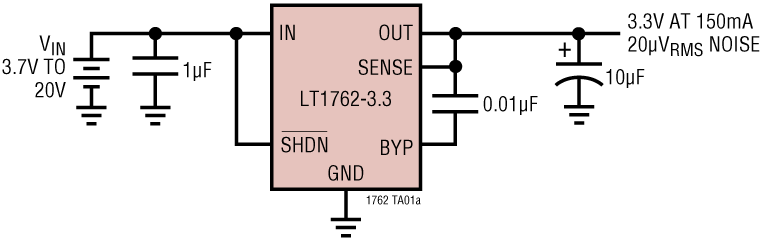
LT1762EMS8 Demo Board | Micropower Low Noise LDO Regulator, 2.3V ≤ VIN ≤ 20V, VOUT = 1.22V/2.5V/3V/3.3V/5V/Adjustable @ 150mA
Analog Devices Inc.Demonstration circuit DC339-A is a low noise micropower voltage regulator using the 150mA output current LT1762 linear regulator in an 8-lead MSOP package. The demo board has an input voltage range from 2.3V to 20V and a jumper-selectable output votlage that can be set to 1.22V, 2.5V, 3.0V, 3.3V, 5V or a user-defined value. The LT1762's low 20µVRMS (10Hz to 100kHz bandwidth) output noise and low 30µA quiescent current make the device ideal for voltage-controlled oscillators, RF power supplies and local regulators in larger systems.

DC342A-A
Analog Devices Inc.The LTC1911 is a switched capacitor step-down DC/DC converter that produces a 1.5V or 1.8V regulated output from a 2.7V to 5.5V input. The part uses switched capacitor fractional conversion to achieve high efficiency over the entire input range. No inductors are required. Internal circuitry controls the step-down conversion ratio to optimize efficiency as the input voltage and load conditions vary. Typical efficiency is over 25% higher than that of a linear regulator.A unique constant frequency architecture provides a low noise regulated output as well as lower input noise than conventional charge pump regulators. High frequency operation (fOSC = 1.5MHz) simplifies output filtering to further reduce conducted noise. To optimize efficiency,the part enters Burst Mode? operation under light load conditions.Low operating current (180?A with no load, 10?A in shutdown) and low external parts count (two 1?F flying capacitors and two 10?F bypass capacitors) make the LTC1911 ideally suited for space constrained battery powered applications. The part is short-circuit and over temperature protected, and is available in an 8-pin MSOP package.Applications Handheld Computers Cellular Phones Smart Card Readers Portable Electronic Equipment Handheld Medical Instruments Low Power DSP Supplies

DC354A
Analog Devices Inc.The LT1768 is designed to control single or multiple cold cathode fluorescent lamp (CCFL) displays. A unique Multimode Dimming scheme* combines both linear and PWM control functions to maximize lamp life, efficiency, and dimming range. Accurate maximum and minimum lamp currents can be easily set. The LT1768 can detect and protect against lamp failures and overvoltage start-up conditions. It is designed to provide maximum flexibility with a minimum number of external components.The LT1768 is a current mode PWM controller with a 1.5A MOSFET driver for high power applications. It contains a 350kHz oscillator, 5V reference, and a current sense comparator with a 100mV threshold. It operates from an 8V to 24V input voltage. The LT1768 also has undervoltage lockout, thermal limit, and a shutdown pin that reduces supply current to 65?A. It is available in a small 16-lead SSOP package.Applications Desktop Flat Panel Displays Multiple Lamp Displays Notebook LCD Displays Point of Sale Terminal Displays

LTC3200EMS8 Demo Board | Regulated Charge Pump White LED Driver, 2.7V ≤ VIN ≤ 4.5V, IOUT Drives 6 Parallel LEDs
Analog Devices Inc.Demonstration Circuit 366A is a low noise constant frequency regulated charge pump featuring the 100mA output current LTC3200. The demo board accepts a 2.7V to 4.5V input voltage and drives six white LEDs in parallel, resulting in 16.6mA per LED. Ballast resistors are employed to provide more uniform light intensity fromr the paralleled LEDs.

DC367A
Analog Devices Inc.The LT1963 series are low dropout regulators optimized for fast transient response. The devices are capable of supplying 1.5A of output current with a dropout voltage of 340mV. Operating quiescent current is 1mA, dropping to

LTC3714EG | Intel's Notebook Processor Power Supply, 7.5V to 24V Input, 0.6V to 1.75VOUT @ 20A
Analog Devices Inc.DC371A: Demo Board for the LTC3714 Intel Compatible, Wide Operating Range, Step-Down Controller with Internal Op Amp.

LTC3778EF | High Efficiency Notebook CPU Power Supply, Ultra Low Voltage Tualatin, VIN = 7.5V - 24V, VCORE = 1.1V/13Amax + VID
Analog Devices Inc.DC389A-C: Demo Board for LTC3778 Wide Operating Range, No RSENSE Step-Down Controller.


