
DC1184A
Analog Devices Inc.The LTC3860 is a dual, PolyPhase? synchronous stepdown switching regulator controller for high current distributed power systems, digital signal processors, and other telecom and industrial DC/DC power supplies. It uses a constant frequency voltage mode architecture combined with very low offset, high bandwidth error amplifiers and a remote output sense differential amplifier for excellent transient response and output regulation. The controller incorporates lossless inductor DCR current sensing to maintain current balance between phases and to provide overcurrent protection. The chip operates from a VCC supply between 3V and 5.5V and is designed for stepdown conversion from VIN between 3V and 24V to output voltages between 0.6V and VCC ? 0.5V. The TRACK/SS pins provide programmable soft-start or tracking functions. Inductor current reversal is disabled during soft-start to safely power prebiased loads. The constant operating frequency can be synchronized to an external clock or linearly programmed from 250kHz to 1.25MHz. Up to six LTC3860 controllers can operate in parallel for 1-, 2-, 3-, 4-, 6- or 12-phase operation. The LTC3860 is available in a 32-pin 5mm ? 5mm QFN package.Applications High Current Distributed Power Systems Digital Signal Processor and ASIC Supplies Telecom Systems Industrial Power Supplies

LTC3850EUF Demo Board | 4.5V ≤ VIN ≤ 14V; VOUT1: 2V @ 10A, VOUT2: 1.8V @ 10A
Analog Devices Inc.Demonstration circuit 1185 is a dual phase/dual output synchronous buck converter featuring the LTC3850EUF. The demo board comes in two versions. The output voltages for version -A are 2.0V/10A and 1.8V/10A and the output voltages for version -B are 1.5V/15A and 1.2V/15A. The input voltage range is 6.5V to 14V for both versions. For applications that have a 5V ±0.5V input, the board has an optional resistor to tie the INTVCC pin to the VIN pin.
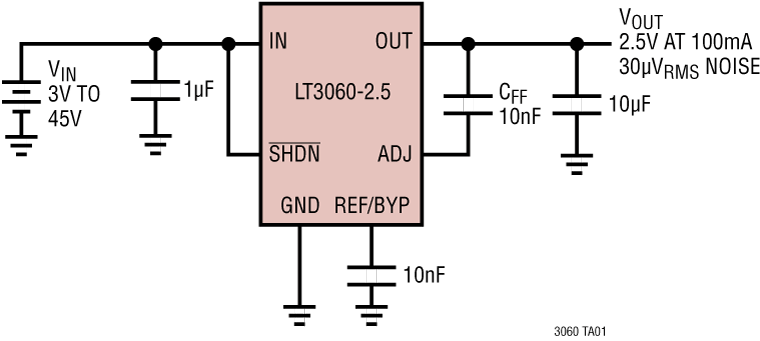
LT3060EDC Demo Board | Low Noise, Low Dropout, Micropower Linear Regulator, 2.1V ≤ VIN ≤ 45V, VOUT = 1.2V/1.5V/1.8V/2.0V/2.5V/3.3V/5V at 100mA
Analog Devices Inc.Demonstration circuit 1209A is a Micropower, low dropout linear regulator featuring LT3060, which comes in an 8-lead TSOT23 or 2mm × 2mm DFN package. The DC1209A has an input voltage range from 2.1V to 45V, and is capable of delivering up to 100mA output current. The jumper-selectable output voltage can be set to 1.2V, 1.5V, 1.8V, 2.0V, 2.5V, 3.3V, 5V or a user-defined value. An external capacitor at REF/BYP pin provides low noise reference and programmable output soft-start functionality. The LT3060’s quiescent current is merely 40µA and provides fast transient response with a minimum 2.2µF output capacitor.

LT3480EDD Demo Board | (DFN) EN55022 Compliant, Micropower, 6.3V ≤ VIN ≤ 38V (60V Transients), VOUT = 5V at 2A
Analog Devices Inc.Demonstration circuit 1212A-A is a monolithic step-down DC/DC switching regulatro featuring the LT3480 in the 3 × 3 DFN-10 package. The demo board provides 5V at 2A from a 6.3V to 38V input and has transient protection up to 60V. The demo boards default switching frequency is 800kHz, but the LT3480 has a SYNC pin which allows frequency synchronization to an external clock over a 250kHz to 2MHz range. The LT3480's quiescent current is 70uA, while the LT3685 has a 0.9mA quiescent current.
An EMC filter at the input makes the circuit compatible with EMC standard EN55022 Class B.

LT3495EDDB Demo Board | 3-6VIN to 15VOUT at 75mA
Analog Devices Inc.Demonstration circuit 1219A-A, A-B, A-C and A-D are micropower low noise boost converters with output disconnect featuring the four different LT3495 versions: LT3495 (0.65A switch current, switching frequency above audible range), LT3495B (0.65A switch current), LT3495-1 (0.35 switch current, switching frequency above audible range) and LT3495B-1 (0.35A switch current). All versions convert a 3V-6V source to 15V. The A-A and A-B versions supply 75mA at 3VIN, while the A-C and A-D supply 36mA.
All versions feature a low noise control scheme, integrated output disconnect function, dimming control and a single output sense resistor.

LT3593DCB | 1MHz White LED Driver with Output Disconnect
Analog Devices Inc.DC1224A: Demo Board for the LT3593 1MHz White LED Driver with Output Disconnect and One Pin Current Programming.

LTC1871EMS-1 Demo Board | SEPIC Controller; 5V to 20 VIN, 12 VOUT @ 3A
Analog Devices Inc.Demonstration circuit 1225 is high efficiency nonisolated SEPIC (Single Ended Primary Inductor Converter) converter featuring the LTC1871-1 switching controller. The DC1225 converts 5V to 20V input to 12V output and provides over 3A of output current. The converter operates at 300kHz with efficiency over 94%. With proper amount of airflow, the DC1225 converter can generate over 3A of output current. The DC1225 can be easily modified to generate output voltages in the range from 1.23V to 48V. Also, the DC1225 can be modified for other input voltages like 5V-36V, 9V-36V, 36V-72V, and so on. The wider input voltage range will decrease the converter efficiency.

LT5579IUH | 456MHz IF, 3.5GHz RF Upconverting Mixer Demo Board
Analog Devices Inc.DC1233A-A: Demo Board for the LT5579 1.5GHz to 3.8GHz High Linearity Upconverting Mixer
LT5579IUH | 456MHz IF, 2.6GHz RF Upconverting Mixer Demo Board
Analog Devices Inc.DC1233A-B: Demo Board for LT5579 1.5GHz to 3.8GHz High Linearity Upconverting Mixer.

DC1235A
Analog Devices Inc.The LTC3826 is a high performance dual step-down switching regulator controller that drives all N-channel synchronous power MOSFET stages. A constant frequency current mode architecture allows a phase-lockable frequency of up to 650kHz. Power loss and noise due to the ESR of the input capacitor are minimized by operating the two controller output stages out of phase.The 30?A no-load quiescent current extends operating life in battery powered systems. OPTI-LOOP compensation allows the transient response to be optimized over a wide range of output capacitance and ESR values. The LTC3826 features a precision 0.8V reference and a power good output indicator. A wide 4V to 36V input supply range encompasses all battery chemistries.Independent TRACK/SS pins for each controller ramp the output voltage during start-up. Current foldback limits MOSFET heat dissipation during short-circuit conditions.The PLLIN/MODE pin selects among Burst Mode operation, pulse skipping mode, or continuous inductor current mode at light loads. For a leaded package version (28-lead SSOP), see the LTC3826-1 data sheet. PGOOD PolyPhase Defeatable Current Foldback Package LTC3826 2 Yes Yes QFN-32 LTC3826-1 1 No No SSOP-28 Applications Automotive Systems Battery-Operated Digital Devices Distributed DC Power Systems

LTC3527EUD-1 Demo Board | Dual, 1.2MHz or 2.2MHz, 0.5V ≤ VIN ≤ 5V, VOUT1 = 3V/3.3V/5V(800mA Switch), VOUT2 = 1.8V/2.85V/3.3V(400mA Switch)
Analog Devices Inc.Demonstration circuit 1237A-A (LTC3527) and 1237A-B (LTC3527-1) are dual output, high-efficiency synchronous boost converter demo boards with each having an 800mA and a 400mA power switch. With a light load, the boost converters can startup with an input voltage as low as 700mV and once started, the input can go as low as 500mV while maintaining a regulated output voltage. Jumpers set the output voltages to one of three options for each output: 3V, 3.3V or 5V for VOUT1, and 1.8V, 2.85V or 3.3V for VOUT2. The devices can provide 200mA at 3.3V from a 1.5V input. The LTC3527-1 actively discharges VOUT1 or VOUT2 when the respective SHDN pin goes low.

LTM8021EV Demoboard | 7.5V ≤ VIN ≤ 36V, VOUT = 5V @ 500mA
Analog Devices Inc.Demonstration circuit 1238B features the LTM8021, a 36V 500mA step-down μModule® regulator. The output has been preset to 5V by a single resistor within the LTM8021’s output voltage range of 0.8V to 5V. An adjustable soft-start period may be implemented with the addition of a capacitor at C3. The input voltage range is from 7.5V to 36V for the default operating conditions. The LTM8021 may need more input voltage to start up than to run in steady state.

LTM4616EV | Low Voltage Dual 8A or Single 16A uModule Regulator
Analog Devices Inc.Demonstration circuit 1245A features the LTM4616, the high efficiency, high density, dual output switch mode power module. The rated load current is 8A for each channel, while derating is necessary for certain VIN, VOUT, and thermal conditions. By applying a clock signal to the CLKIN pin, the module’s switching frequency may be synchronized from 0.75MHz to 2.25MHz. The same clock frequency is available at the CLKOUT pin with the phase relationship between CLKIN and CLKOUT determined by the PHMODE pin. This feature can be used not only to reduce undesirable frequency harmonics but also to parallel the two channels of LTM4616 or even multiple LTM4616s and LTM4608s to provide higher output currents.

LTC1606ACG Demo Board | 16-Bit, 250ksps ADC (Requires DC718 Controller)
Analog Devices Inc.DC1255A-B: Demo Board for the LTC1606 16-Bit, 250ksps, Single Supply ADC

LTC2209UP | High IF, LVDS Out, 160Msps, 16-Bit ADC, 1MHz < Ain <80MHz, (requires DC890 & LVDS_XFMR)
Analog Devices Inc.DC1281A-A: Demo Board for LTC2209 16-Bit, 160Msps ADC

DC1285A
Analog Devices Inc.The LT3598 is a fixed frequency step-up DC/DC converter designed to drive up to six strings of LEDs at an output voltage up to 44V. LED dimming can be achieved with analog dimming on the CTRL pin, and with pulse width modulation dimming on the PWM pin. The LT3598 accurately regulates LED current even when the input voltage is higher than the LED output voltage. The switching frequency is programmable from 200kHz to 2.5MHz through an external resistor. Additional features include programmable overvoltage protection, switching frequency synchronization to an external clock, LED current derating based on junction temperature and/or LED temperature, LED string disable control, OPENLED alert pin and output voltage limiting when all LED strings are disconnected. The LT3598 is available in a thermally enhanced 24-lead (4mm ? 4mm) QFN and 24-lead TSSOP packages.Applications Notebook Computer Display Medium Size Displays Automotive LCD Display

LTC3775EUD Demo Board | 5V ≤ VIN ≤ 36V, VOUT = 1.2V @ 10A
Analog Devices Inc.Demonstration circuit 1290A is a high frequency synchronous step-down converter featuring the LTC3775EUD. The package style for the LTC3775EUD is a 16-pin 3mm x 3mm QFN. Two versions of the demonstration board are available. DC-1290A-A has been optimized for 5V to 26V input and typically provides 1.2V/15A, while the DC1290A-B is optimized for 5V to 36VIN range and typically provides 1.2V/10A.

DC1295B
Analog Devices Inc.The LTM4606 is a complete EN55022 Class B certified noise high voltage 6A switching mode DC/DC power supply. Included in the package are the switching controller, power FETs, inductor, and all support components. The on-board input filter and noise cancellation circuits achieve low noise operation, thus effectively reducing the electromagnetic interference (EMI). Operating over an input voltage range of 4.5V to 28V, the LTM4606 supports an output voltage range of 0.6V to 5V, set by a single resistor. This high efficiency design delivers 6A continuous current (8A peak). Only bulk input and output capacitors are needed to finish the design.High switching frequency and an adaptive on-time current mode architecture enables a very fast transient response to line and load changes without sacrificing stability. The device supports output voltage tracking and output voltage margining.Furthermore, the ?Module? regulator can be synchronized with an external clock for reducing undesirable frequency harmonics and allows PolyPhase? operation for high load currents.The LTM4606 is offered in space saving 15mm ? 15mm ? 2.82mm LGA and 15mm ? 15mm ? 3.42mm BGA packages. The LTM4606 is available with SnPb (BGA) or RoHS compliant terminal finish.APPLICATIONS ASICs or FPGA Transceivers Telecom, Servers and Networking Equipment Industrial Equipment RF Equipment

DC1299A-A
Analog Devices Inc.The LTC6420-20 is a dual high-speed differential amplifier targeted at processing signals from DC to 300MHz. The part has been specifically designed to drive 12-, 14- and 16-bit ADCs with low noise and low distortion, but can also be used as a general-purpose broadband gain block.The LTC6420-20 is easy to use, with minimal support circuitry required. The output common mode voltage is set using an external pin, independent of the inputs, which eliminates the need for transformers or AC-coupling capacitors in many applications. The gain is internally fixed at 20dB (10V/V).The LTC6420-20 saves space and power compared to alternative solutions using IF gain blocks and transformers. The LTC6420-20 is packaged in a compact 20-lead 3mm ? 4mm QFN package and operates over the ?40?C to 85?C temperature range.Applications Differential ADC Driver Single Ended to Differential Conversion IF Sampling (Diversity) Receivers Broadband I/Q Amplifiers Satellite Communications

LTC3725EMSE/LTC3726EGN 1/4 Brick | 9V < VIN < 36V, VOUT: 5.0V/20A
Analog Devices Inc.DC1300A-A: Demo Board for:
LTC3725 - Single-Switch Forward Controller and Gate Driver
LTC3726 - Secondary-Side Synchronous Forward Controller


