
ADL5566-EVALZ
Analog Devices Inc.The ADL5566 is a high performance, dual differential amplifier optimized for IF and dc applications. The amplifier offers low noise of 1.3 nV/?Hz and excellent distortion performance over a wide frequency range, making it an ideal driver for high speed 16-bit analog-to-digital converters (ADCs). The ADL5566 is ideally suited for use in high performance, zero IF/complex IF receiver designs. In addition, this device has excellent low distortion for single-ended input drive applications.The ADL5566 provides a gain of 16 dB. For the single-ended input configuration, the gain is reduced to 14 dB. Using two external series resistors for each amplifier expands the gain flexibility of the amplifier and allows for any gain selection from 0 dB to 16 dB for a differential input and 0 dB to 14 dB for a single-ended input. In addition, this device maintains low distortion down to output (VOCM) levels of 1.2 V providing an added capability for driving CMOS ADCs at ac levels up to 2 V p-p.The quiescent current of the ADL5566, using a 3.3 V supply, is typically 70 mA per amplifier. When disabled, it consumes less than 3.5 mA per amplifier and has ?25 dB of input to output isolation at 100 MHz.The device is optimized for wideband, low distortion, and noise performance, giving it unprecedented performance for overall spurious-free dynamic range (SFDR). These attributes, together with the adjustable gain capability, make this device the amplifier of choice for driving a wide variety of ADCs, mixers, pin diode attenuators, SAW filters, and multi-element discrete devices.Fabricated on an Analog Devices, Inc., high speed SiGe process, the ADL5566 is supplied in a compact 4 mm ? 4 mm, 24-lead LFCSP package and operates over the ?40?C to +85?C temperature range.Applications Differential ADC drivers Single-ended to differential conversion RF/IF gain blocks SAW filter interfacing

ADL5567-EVALZ
Analog Devices Inc.The ADL5567 is a high performance, dual differential amplifieroptimized for intermediate frequencies (IF) and dc applications.The amplifier offers a low noise of 1.29 nV/?Hz and excellentdistortion performance over a wide frequency range, making itan ideal driver for high speed 16-bit analog-to-digital converters(ADCs). The ADL5567 is ideally suited for use in high performancezero-IF and complex IF receiver designs. In addition, this devicehas excellent low distortion for single-ended input driverapplications.The ADL5567 provides a gain of 20 dB. For the single-ended inputconfiguration, the gain is reduced to 18 dB. Using two externalseries resistors for each amplifier expands the gain flexibility ofthe amplifier and allows for any gain selection from 0 dB to 20 dBfor a differential input and 0 dB to 18 dB for a single-ended input.In addition, this device maintains low distortion down to outputcommon-mode levels of 1.25 V, and therefore providing an addedcapability for driving CMOS ADCs at ac levels up to 2 VP-P.The quiescent current of the ADL5567 using a 5 V supply istypically 74 mA per amplifier in high performance mode.When disabled, each amplifier consumes only 3.5 mA, and has58 dB input to output isolation at 100 MHz.The device is optimized for wideband, low distortion, and lownoise operation, giving it unprecedented performance foroverall spurious-free dynamic range (SFDR). These attributes,together with its adjustable gain capability, make this device theamplifier of choice for driving a wide variety of ADCs, mixers,pin diode attenuators, SAW filters, and multielement discretedevices.Fabricated on an Analog Devices, Inc., high speed silicongermanium (SiGe) process, the ADL5567 is supplied in acompact 4 mm ? 4 mm, 24-lead LFCSP package and operatesover the ?40?C to +85?C temperature.APPLICATIONS Differential ADC drivers Single-ended to differential conversions RF/IF gain blocks SAW filter interfacing

ADL5580-EVALZ
Analog Devices Inc.The ADL5580 is a high performance, single-ended or differential amplifier with 10 dB of voltage gain, optimized for applications spanning from dc to 10.0 GHz. The amplifier offers a low referred to input (RTI) noise spectral density (NSD) of 2.24 nV/?Hz (at 1000 MHz) and is optimized for distortion performance over a wide frequency range, making the device an ideal driver for high speed 12-bit to 16-bit analog-to-digital converters (ADCs). The ADL5580 is suited for use in high performance, zero intermediate frequency (IF), and complex IF receiver designs. In addition, this device has low distortion for single-ended input driver applications.By using two external series resistors, the gain selection from 10 dB for a differential input can be modified to a lower gain. The device maintains low distortion through its output common-mode voltage (VCM) of 0.5 V, providing a flexible capability for driving ADCs with full-scale levels up to 1.4 V p-p.Operating from a +5 V and ?1.8 V supply, the positive and negative supply current of the ADL5580 is typically +276 mA and ?224 mA, respectively. The device has a power disable feature, and when disabled, the amplifier consumes 2 mA.The ADL5580 is optimized for wideband, low distortion, and low noise operation at the dc to 10.0 GHz frequency range. These attributes, together with its adjustable gain capability, make this device an optimal choice for driving a wide variety of ADCs, mixers, pin diode attenuators, surface acoustic wave (SAW) filters, and a multiplicity of discrete RF devices.Fabricated on an Analog Devices, Inc., high speed silicon germanium (SiGe) process, the ADL5580 is supplied in a compact 4 mm ? 4 mm, 20-terminal land grid array (LGA)package and operates over the ?40?C to +85?C temperature range.APPLICATIONSInstrumentation and defense applications

ADL5601-EVALZ
Analog Devices Inc.The ADL5601 is a broadband, 15 dB linear amplifier that operates at frequencies up to 4.0 GHz. The device can be used in a wide variety of cellular, cable television (CATV), military, and instru-mentation equipment.The ADL5601 provides the highest dynamic range available from an internally matched gain block. This is accomplished by providing extremely low noise figures and very high OIP3 speci-fications simultaneously, across the entire 4.0 GHz frequency range.The ADL5601 provides a gain of 15 dB, which is stable over frequency, temperature, and supply voltage, as well as from device to device. The device is internally matched to 50 ? at the input and output, making the ADL5601 very easy to implement in a wide variety of applications. Only input/output ac coupling capacitors, power supply decoupling capacitors, and an external inductor are required for operation.The ADL5601 is fabricated on an InGaP heterojunction bipolar transistor (HBT) process and has an ESD rating of ?1.5 kV (Class 1C). The device is available in a thermally efficient SOT-89 package.The ADL5601 consumes 83 mA on a single 5 V supply and is fully specified for operation from ?40?C to +85?C.A fully populated RoHS-compliant evaluation board is available.

ADL5602-EVALZ
Analog Devices Inc.The ADL5602 is a broadband 20 dB linear amplifier that operates at frequencies up to 4 GHz. The device can be used in a wide variety of cellular, CATV, military, and instrumentation equipment.The ADL5602 provides the highest dynamic range available from an internally matched gain block. This is accomplished by providing extremely low noise figures and very high OIP3 specifications simultaneously, across the entire 4 GHz frequency range.The ADL5602 provides a gain of 20 dB, which is stable over frequency, temperature, power supply, and from device to device. The device is internally matched to 50 ? at the input and output, making the ADL5602 very easy to implement in a wide variety of applications. Only input/output ac coupling capacitors, power supply decoupling capacitors, and an external inductor are required for operation.The ADL5602 is fabricated on an InGaP HBT process and has an ESD rating of ?1.5 kV (Class 1C). The device is available in a thermally efficient SOT-89 package.The ADL5602 consumes 89 mA on a single 5 V supply and is fully specified for operation from ?40?C to +85?C.A fully populated RoHS-compliant evaluation board is available.
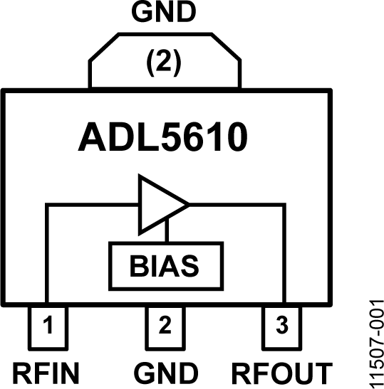
ADL5610-EVALZ
Analog Devices Inc.The ADL5610 is a single-ended RF/IF gain block amplifier that provides broadband operation from 30 MHz to 6 GHz. The ADL5610 provides a low noise figure of 2.2 dB with a very high OIP3 of more than 38 dBm simultaneously, which delivers a high dynamic range.?The ADL5610 provides a gain of 18 dB, which is stable over frequency, temperature, and power supply, and from device to device. The amplifier is offered in the industry-standard SOT-89 package and is internally matched to 50 ? at the input and output, making the ADL5610 easy to implement in a wide variety of applications. The only external parts required are the input and output ac coupling capacitors, power supply decoupling capacitors, and bias inductor.The ADL5610 has a high ESD rating of ?1.5 kV (Class 1C) and is fully specified for operation across a wide temperature range of ?40?C to +105?C.?A fully populated RoHS-compliant evaluation board is available.

ADL5611-EVALZ
Analog Devices Inc.The ADL5611 is a single-ended RF/IF gain block amplifier that provides broadband operation from 30 MHz to 6 GHz. The ADL5611 provides a low noise figure of 2.1 dB with a very high OIP3 of 40.0 dBm simultaneously, which delivers a high dynamic range.The ADL5611 provides a gain of 22.2 dB that is stable over frequency, temperature, and power supply, and from device to device. The amplifier is offered in the industry-standard SOT-89 package and is internally matched to 50?? at the input and output, making the ADL5611 easy to implement in a wide variety of applications. The only external parts required are the input and output ac coupling capacitors, power supply decoupling capacitors, and bias inductor.The ADL5611 has a high ESD rating of ?1.5 kV (Class 1C) and is fully specified for operation across a wide temperature range of ?40?C to +105?C. A fully populated RoHS-compliant evaluation board is available.

DC1124A
Analog Devices Inc.The LT3591 is a fixed frequency step-up DC/DC converter speci?cally designed to drive up to ten white LEDs in series from a Li-Ion cell. Series connection of the LEDs provides identical LED currents resulting in uniform brightness and eliminating the need for ballast resistors. The device features a unique high side LED current sense that enables the part to function as a ?one wire current source;? one side of the LED string can be returned to ground anywhere, allowing a simpler one wire LED connection. Traditional LED drivers use a grounded resistor to sense LED current, requiring a 2-wire connection to the LED string.The high switching frequency allows the use of tiny inductors and capacitors. A single pin performs both shutdown and accurate LED dimming control. Few external components are needed: open-LED protection and the Schottky diode are all contained inside a low pro?le 3mm ? 2mm DFN package.Applications Tape and Reel: Add #TR Lead Free: Add #PBF Lead Free Tape and Reel: Add #TRPBF

LT5557EUF | 400MHz to 3.8GHz 3.3V Down Mixer, 1.95GHz RFin, 240MHz Balun IF Out
Analog Devices Inc.DC1131A: Demo Board for the LT5557 400MHz to 3.8GHz 3.3V Active Downconverting Mixer.

LTC4222 Demoboard | Dual Hot Swap Controller with I2C and ADC (Requires DC590)
Analog Devices Inc.DC1134A: Demo Board for LTC4222 Dual Hot Swap Controller with I2C Compatible Monitoring

LTC6404-1 Demo Circuit
Analog Devices Inc.DC1147A-A: Demo Board for the LTC6404 600MHz, Low Noise, High Precision Fully Differential Input/Output Amplifier/Driver
LTC6404-4 Demo Circuit
Analog Devices Inc.DC1147A-C: Demo Board for the LTC6404 600MHz, Low Noise, High Precision Fully Differential Input/Output Amplifier/Driver

DC1150A
Analog Devices Inc.The LT5554 is a 7-bit digitally controlled programmable gain (PG) amplifier with 16dB gain control range. It consists of a 50? input variable attenuator, followed by a high linearity variable transconductance amplifier. The coarse 4dB input attenuator step is implemented via 2-bits of digital control (PG5, PG6). The ?ne transconductance amplifier 0.125dB step within 3.875dB gain control range is set via 5-bits digital control (PG0 to PG4). The LT5554 gain control inputs (PGx) and the STROBE input can be directly coupled to TTL or ECL drivers. The seven parallel gain control inputs time skew can be eliminated by using the STROBE input positive transition.The internal output resistor RO = 400? limits the maximum overall gain to 36dB for open outputs. The internal circuitry of open output collectors enables the LT5554 to be unconditionally stable over any loading conditions (including external SAW ?lters) and provides ?80dB reverse isolation at 300MHz.The LT5554 is internally protected during overdrive and has an on-chip power supply regulator.With 0.125dB step resolution and 5ns settling time, the LT5554 is suitable in applications where continuous gain control is required.Applications Differential ADC Driver IF Sampling Receivers VGA IF Power Ampli?er 50? Driver Instrumentation

LTC3780EUH Demo Board | Synchronous Buck-Boost Controller
Analog Devices Inc.Demonstration circuit 1155A is a compact high efficiency synchronous buck-boost DC/DC converter solution featuring the LTC3780EUH controller. with 6V to 32V input range. It can supply 2A maximum load current at 12V output. The constant frequency current mode architecture allows a phase-lockable frequency of up to 400kHz.

LT3518EUF Demo Board
Analog Devices Inc.DC1160A: Demo Board for LT3518 Full-Featured LED Driver with 2.3A Switch Current

LT3507EUHF Demo Board | 7V to 36VIN, VOUT1 = 1.8V @ 2.4A, VOUT2 = 3.3V @ 1.3A, VOUT3 = 5.0V @ 1.4A, VOUT4 = 2.5V @ 0.2A
Analog Devices Inc.Demo circuit 1161B is a triple monolithic step-down regulator with LDO featuring LT3507. The demo circuit is designed for 1.8V, 3.3V, 5.0V and 2.5V outputs from a 7V to 36V input. The current capability of each channel is 2.4A, 1.3A, 1.4A and 0.2A respectively. Independent input voltage, feedback, soft-start and power good pins for each channel simplify complex power supply tracking/sequencing requirements.
All three converters are either synchronized to a common external clock input or single-resistor programmable from 250kHz to 2.5MHz using internal oscillator. At all frequencies, a 180° phase shift between VOUT1 and the other two outputs is maintained, reducing input voltage ripple and component size. Programmable frequency allows for optimization between efficiency and external component size.

LT3590EDC Demo Board | Buck Mode LED Driver, Tiny Package, 4.5V ≤ VIN ≤ 54V, VLED up to 40V at 50mA
Analog Devices Inc.Demonstration circuit 1166 is a 48V Buck-Mode LED Driver featuring the LT3590. The LT3590 is a fixed frequency buck mode converter specifically designed to drive up to 10 LEDs in series at up to 50mA LED current. Series connection of the LEDs results in uniform LED brightness, eliminating the need for ballast resistors. The demo board targets 48V power applications but has a wide 4.5V to 54V (55V absolute max) input voltage range.

LTC3851EGN (DCR) Demo Board | 4.5V < VIN < 14V, VOUT: 1.5V/15A
Analog Devices Inc.DC1171A-B: Demo Board for the LTC3851 Synchronous Step-Down Switching Regulator Controller

LTC3725EMSE/LTC3726EGN 1/8 Brick | 9V < VIN < 36V, VOUT: 5.0V/10A
Analog Devices Inc.DC1174A-A: Demo Board for the LTC3725 Single-Switch Forward Controller and Gate Driver and LTC3726 Secondary-Side Synchronous Forward Controller

DC1178A
Analog Devices Inc.The LT5568-2 is a direct I/Q modulator designed for high performance wireless applications, including wireless infrastructure. It allows direct modulation of an RF signal using differential baseband I and Q signals. It supports GSM, EDGE, CDMA, CDMA2000 and other systems that operate in the 850MHz to 965MHz band. It may be configured as an image reject upconverting mixer, by applying 90? phase-shifted signals to the I and Q inputs. The I/Q baseband inputs consist of voltage-to-current converters that in turn drive double-balanced mixers. The outputs of these mixers are summed and applied to an on-chip RF transformer, which converts the differential mixer signals to a 50? single-ended output. The four balanced I and Q baseband input ports are intended for DC coupling from a source with a common mode voltage level of about 0.5V. The LO path consists of an LO buffer with single-ended input, and precision quadrature generators that produce the LO drive for the mixers. The supply voltage range is 4.5V to 5.25V.Applications Infrastructure Tx for GSM/Cellular Bands Image Reject Up-Converters for Cellular Bands Low-Noise Variable Phase-Shifter for 700MHz to 1050MHz Local Oscillator Signals RFID Reader


