
DC2026C-KIT
Analog Devices Inc.The LTC2607/LTC2617/LTC2627 are dual 16-, 14- and 12-bit, 2.7V to 5.5V rail-to-rail voltage output DACs in a 12-lead DFN package. They have built-in high performance output buffers and are guaranteed monotonic.These parts establish new board-density benchmarks for 16- and 14-bit DACs and advance performance standards for output drive and load regulation in single-supply, voltage-output DACs.The parts use a 2-wire, I2C compatible serial interface. The LTC2607/LTC2617/LTC2627 operate in both the standard mode (clock rate of 100kHz) and the fast mode (clock rate of 400kHz). An asynchronous DAC update pin (LDAC) is also included.The LTC2607/LTC2617/LTC2627 incorporate a power-on reset circuit. During power-up, the voltage outputs rise less than 10mV above zero scale; and after power-up, they stay at zero scale until a valid write and update take place. The power-on reset circuit resets the LTC2607-1/LTC2617-1/ LTC2627-1 to mid-scale. The voltage outputs stay at midscale until a valid write and update takes place.Applications Mobile Communications Process Control and Industrial Automation Instrumentation Automatic Test Equipment

LTC4364DE-1 Demoboard: 12V Surge Stopper with Ideal Diode, Latch Off
Analog Devices Inc.DC2027A-A: Demo Board for the LTC4364 Surge Stopper with Ideal Diode.

DC2028A
Analog Devices Inc.The LTC2977 is an 8-channel Power System Manager used to sequence, trim (servo), margin, supervise, manage faults, provide telemetry and create fault logs. PMBus commands support power supply sequencing, precision point-of-load voltage adjustment and margining. DACs use a proprietary soft-connect algorithm to minimize supply disturbances. Supervisory functions include overvoltage and undervoltage threshold limits for eight power supply output channels and one power supply input channel, as well as over and under temperature limits. Programmable fault responses can disable the power supplies with optional retry after a fault is detected. Faults that disable a power supply can automatically trigger black box EEPROM storage of fault status and associated telemetry. An internal 16-bit ADC monitors eight output voltages, one input voltage, and die temperature. In addition, odd numbered channels can be configured to measure the voltage across a current sense resistor. A programmable watchdog timer monitors microprocessor activity for a stalled condition and resets the microprocessor if necessary. A single wire bus synchronizes power supplies across multiple LTC Power System Management (PSM) devices. Configuration EEPROM with ECC supports autonomous operation without additional software.APPLICATIONS Computers and Network Servers Industrial Test and Measurement High Reliability Systems Medical Imaging Video

DC2038A-H
Analog Devices Inc.The LTC4162-S is an advanced monolithic synchronous step-down switching battery charger and PowerPath? manager that seamlessly manages power distribution between input sources such as wall adapters, backplanes, solar panels, etc., and a lead-acid battery.A high resolution measurement system provides extensive telemetry information for circuit voltages, currents, battery resistance and temperature which can all be read back over the I2C port. The I2C port can also be used to configure many charging parameters including charging voltages and currents, termination algorithms and numerous system status alerts.The LTC4162-S can charge 6V, 12V, 18V and 24V lead-acid batteries with as much as 3.2A of charge current.The power path topology decouples the output voltage from the battery allowing a portable product to start up instantly under very low battery voltage conditions.The LTC4162-S is available in a thermally enhanced 28-pin 4mm ? 5mm ? 0.75mm QFN surface mount package.Applications Medical Instruments USB-C Power Delivery Industrial Handhelds Ruggedized Notebook Tablet Computers

LT4276B/LT4321 Demo Board | PoE+(25W, 24V/1A) PD with DC/DC and Ideal Diode Bridge
Analog Devices Inc.Demonstration circuit 2046A-D is a PoE powered device (PD) with an isolated power supply using synchronous flyback topology, featuring the LT4276 and ideal diode bridge controller (LT4321).
LT4276B/LT4321 Demo Board | PoE+ (25W, 12V/1.9A) PD with DC/DC, Ideal Diode Bridge and 9V-57V AUX
Analog Devices Inc.Demonstration circuit 2047A-A is an IEEE802.3at compliant Power over Ethernet (PoE) Powered Device (PD) with support for 9-57VDC and 24VAC auxiliary supply input. It features the LT4276 PD interface and switching regulator controller, the LT4321 PoE ideal diode bridge controller, and the LT4320 ideal diode bridge controller.

LT1776CS8 | High Voltage, High Efficiency, Step-Down Switching Regulator, 7V to 60VIN, 3.3V and 5V @ 0.5A Out (Thru-hole Input Cap)
Analog Devices Inc.DC204A-B: Demo Board for the LT1776 Wide Input Range, High Efficiency, Step-Down Switching Regulator.

DC2050A
Analog Devices Inc.The LT3753 is a current mode PWM controller optimized for an active clamp forward converter topology, allowing up to 100V input operation.A programmable volt-second clamp allows primary switch duty cycles above 50% for high switch, transformer and rectifier utilization. Active clamp control reduces switch voltage stress and increases efficiency. A synchronous output is available for controlling secondary side synchronous rectification.The LT3753 is available in a 38-lead plastic TSSOP package with missing pins for high voltage spacings.Applications Industrial, Automotive and Military Systems 48V Telecommunication Isolated Power Supplies

LT4363IDE-1 Demo Board: 12V System ISO-7637-2 Surge Stopper, Latch-Off Version
Analog Devices Inc.DC2062A-A: Demo Board for LT4363 High Voltage Surge Stopper with Current Limit.

DC2066A
Analog Devices Inc.The LTM4677 is a dual 18A or single 36A step-down ?Module? (power module) DC/DC regulator with 40ms turn0on time. It features remote configurability and telemetry-monitoring of power management parameters over PMBus?an open standard I2C-based digital interface protocol. The LTM4677 is comprised of fast analog control loops, precision mixedsignal circuitry, EEPROM, power MOSFETs, inductors and supporting components.The LTM4677?s 2-wire serial interface allows outputs to be margined, tuned and ramped up and down at programmable slew rates with sequencing delay times. Input and output currents and voltages, output power, temperatures, uptime and peak values are readable. Custom configuration of the EEPROM contents is not required. At start-up, output voltages, switching frequency, and channel phase angle assignments can be set by pin-strapping resistors. The LTpowerPlay? GUI and DC1613 USB-to-PMBus converter and demo kits are available.The LTM4677 is pin compatible with the LTM4676A (dual 13A) and is offered in a 16mm ? 16mm ? 5.01mm BGA package available with SnPb or RoHS compliant terminal finish.APPLICATIONS System Optimization, Characterization and Data Mining?in Prototype, Production and Field Environments Telecom, Datacom, and Storage Systems

DC2071A-B
Analog Devices Inc.The LTC2372-18 is a low noise, high speed, 8-channel 18-bit successive approximation register (SAR) ADC. Operating from a single 5V supply, the LTC2372-18 has a highly configurable, low crosstalk 8-channel input multiplexer, supporting fully differential, pseudo-differential unipolar and pseudo-differential bipolar analog input ranges. The LTC2372-18 achieves ?2.75LSB INL (maximum) in all input ranges, no missing codes at 18-bits and 100dB (fully differential)/ 95dB (pseudo-differential) SNR (typical).The LTC2372-18 has an onboard low drift (20ppm/?C max) 2.048V temperature-compensated reference and a single-shot capable reference buffer. The LTC2372-18 also has a high speed SPI-compatible serial interface that supports 1.8V, 2.5V, 3.3V and 5V logic through which a sequencer with a depth of 16 may be programmed. An internal oscillator sets the conversion time, easing external timing considerations. The LTC2372-18 dissipates only 27mW and automatically naps between conversions, leading to reduced power dissipation that scales with the sampling rate. A sleep mode is also provided to reduce the power consumption of the LTC2372-18 to 300?W for further power savings during inactive periods.Applications Programmable Logic Controllers Industrial Process Control High Speed Data Acquisition Portable or Compact Instrumentation ATE

LT1725IGN | 48VIN to 5VOUT 2A Module, Isolated Flyback, 1x2 Footprint
Analog Devices Inc.DC373A-A: Demo Board for the LT1725 General Purpose Isolated Flyback Controller.

LTC3716EG | 2-Phase Mobile CPU VRM, 7 to 24VIN, 0.6 to 1.75VOUT @ 25A (maximum performance)
Analog Devices Inc.DC377B-A: Demo Board for the LTC3716 - 2-Phase, 5-Bit VID, Current Mode, High Efficiency, Synchronous Step-Down Switching Regulator
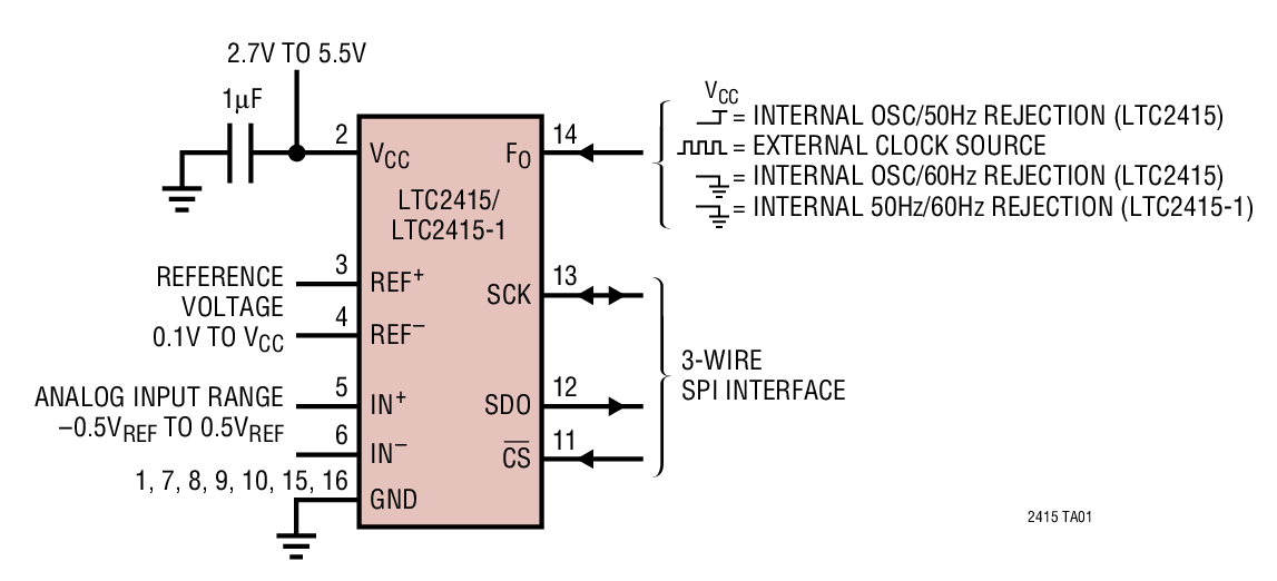
LTC2415CGN | Differential Input 24-Bit ADC with 2X Output Rate (with Diskette, Requires Win95/98)
Analog Devices Inc.DC382A: Demo Board for LTC2415 24-Bit No Latency Delta Sigma ADC with Differential Input and Differential Reference.

LTC3778EF | High Efficiency Notebook CPU Power Supply, Mobile Tualatin, VIN = 7.5V - 24V, VCORE = 1.4V/23Amax + VID
Analog Devices Inc.DC389A-A: Demo Board for LTC3778: Wide Operating Range, No RSENSE Step-Down Controller.

LTC3728EUH Demo Board | Dual Output, 5V to 24VIN, 5VOUT1 @ 4A, 3.3VOUT2 @ 5A
Analog Devices Inc.Demonstration circuit 392 is a dual output, step-down, synchronous buck converter featuring either the 150kHz to 300kHz LTC1628EUH controller (DC392A-A), the 250kHz to 550kHz LTC3728EUH (DC392A-B) or 250kHz to 550kHz LTC3728LUH (DC392A-C). It operates with an input voltage range of 7V to 24V and provides 3.3V @ 5A and 5V @ 4A at its output.

LT1930AES5/LT1931AES5 Demo Board | 3 Circuits: Boost/SEPIC/Inverter: 5VIN to 12VOUT1 @ 250mA, 10V-16VIN to 12VOUT2 @ 250mA, 12VIN to -12VOUT3 @ 250mA
Analog Devices Inc.Demonstration circuit 397 is a multipurpose DC/DC switching regulator using the LT1930A and LT1931A voltage regulators in a SOT-23 package. The demo board offers three separate DC/DC converters for different applications needs. The boost circuit is designed to convert a 5V input to 12V output at 250mA maximum load. The SEPIC circuit generates a constant 12V/250mA (max load) output with a 10V~16V variable input. The inverter circuit is de-signed for applications requiring negative 12V/250mA (max load) from a positive 12V input. All three circuits are designed to demonstrate fast switching frequency (2.2MHz), an internal 36V/1A switch, wide input range, and small circuit size.

LTC3400ES6 | 1.2MHz, High Efficiency Synchronous Boost Converter, VIN = 1V to 3V, VOUT = 3.3V @ 90mA
Analog Devices Inc.DC398A-A: Demo Board for LTC3400 600mA, 1.2MHz Micropower Synchronous Boost Converters in ThinSOT.

LTC3402EMS | Synchronous Boost Converter, VIN=1 to 4.5V, VOUT=3.3V or 5V
Analog Devices Inc.DC409A: Demo Board for the LTC3402 2A, 3MHz Micropower Synchronous Boost Converter

DC413A
Analog Devices Inc.The LTC3404 is a high efficiency monolithic synchronous buck regulator using a constant frequency, current mode architecture. Supply current during operation is only 10?A and drops to < 1?A in shutdown. The 2.65V to 6V input voltage range makes the LTC3404 ideally suited for single Li-Ion battery-powered applications. 100% duty cycle provides low dropout operation, extending battery life in portable systems.Switching frequency is internally set at 1.4MHz, allowing the use of small surface mount inductors and capacitors. For noise sensitive applications the LTC3404 can be externally synchronized from 1MHz to 1.7MHz. Burst Mode operation is inhibited during synchronization or when the SYNC/MODE pin is pulled low, preventing low frequency ripple from interfering with audio circuitry. The internal synchronous switch increases efficiency and eliminates the need for an external Schottky diode. Low output voltages are easily supported with the 0.8V feedback reference voltage. The LTC3404 is available in a space saving 8-lead MSOP package. For higher input voltage (11V abs max) applications, refer to the LTC1877 data sheet.Applications Cellular Telephones Wireless and DSL Modems Personal Information Appliances Portable Instruments Distributed Power Systems Battery-Powered Equipment


