
DC769A
Analog Devices Inc.The LTC3808 is a synchronous step-down switching regulator controller that drives external complementary power MOSFETs using few external components. The constant frequency current mode architecture with MOSFET VDS sensing eliminates the need for a current sense resistor and improves efficiency.Burst Mode operation provides high efficiency operation at light loads. 100% duty cycle provides low dropout operation, extending operating time in battery-powered systems.The switching frequency can be programmed up to 750kHz, allowing the use of small surface mount inductors and capacitors. For noise sensitive applications, the LTC3808 can be externally synchronized from 250kHz to 750kHz. Burst Mode is inhibited during synchronization or when the SYNC/MODE pin is pulled low to reduce noise and RF interference. To further reduce EMI, the LTC3808 incorporates a novel spread spectrum frequency modulation technique.The LTC3808 is available in the tiny footprint thermally enhanced DFN package or 16-lead SSOP package.Protected by U.S. Patents including 5481178, 5929620, 6580258, 6304066, 5847554, 6611131, 6498466. Other Patents pending. Features Package LTC3809 PLL, Selectable Spread Spectrum, Power Good 3x3 DFN-10, MS-10E LTC3809-1 Tracking 3x3 DFN-10, MS-10E LTC3808 PLL, Selectable Spread Spectrum, Tracking Power Good 4x3 DFN-14, SSOP-16 Applications One or Two Cell Lithium-Ion Powered Devices Notebook and Palmtop Computers, PDAs Portable Instruments Distributed DC Power Systems

LTC2239IUH | High Speed ADC, VDD = +3.0V, 80Msps, 10-Bit 1MHz < AIN < 70MHz, Requires DC718
Analog Devices Inc.DC782A-L: Demo Board for the LTC2239 10-Bit, 80Msps Low Noise 3V ADC.

DC782A-U
Analog Devices Inc.The LTC2253/LTC2252 are 12-bit 125Msps/105Msps, low power 3V A/D converters designed for digitizing high frequency, wide dynamic range signals. The LTC2253/LTC2252 are perfect for demanding imaging and communications applications with AC performance that includes 70.1dB SNR and 85dB SFDR for signals at the Nyquist frequency.DC specs include ?0.3LSB INL (typ), ?0.15LSB DNL (typ) and no missing codes over temperature. The transition noise is a low 0.32LSBRMS.A single 3V supply allows low power operation. A separate output supply allows the outputs to drive 0.5V to 3.3V logic.A single-ended CLK input controls converter operation. An optional clock duty cycle stabilizer allows high performance at full speed for a wide range of clock duty cycles.Applications Wireless and Wired Broadband Communication Imaging Systems Ultrasound Spectral Analysis Portable Instrumentation
DC786A
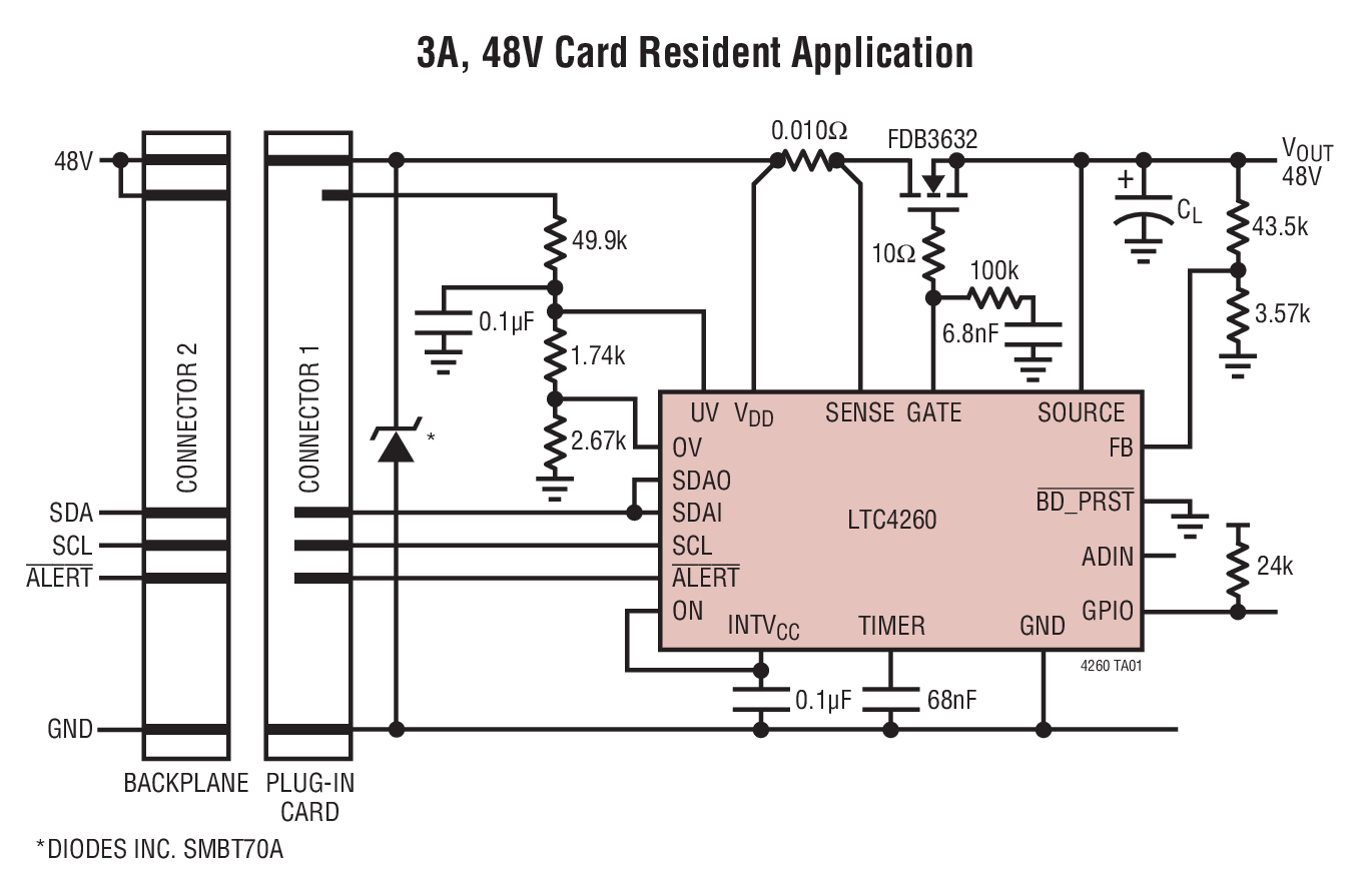
Analog Devices Inc.The LTC4260 Hot Swap? controller allows a board to be safely inserted and removed from a live backplane. Using an external N-channel pass transistor, the board supply voltage can be ramped up at an adjustable rate. An I2C interface and onboard ADC allow monitoring of board current, voltage and fault status.The device features adjustable analog foldback current limit with latch off or automatic restart after the LTC4260 remains in current limit beyond an adjustable time-out delay.The controller has additional features to interrupt the host when a fault has occurred, notify when output power is good, detect insertion of a load card and power-up in either the on or off state.Applications Electronic Circuit Breakers Live Board Insertion Computers, Servers

LTC2439CGN-1 | 8-Channel Differential 16-Bit ADC (Requires DC590)
Analog Devices Inc.DC790A: Demo Board for the LTC2439-1 8-/16-Channel 16-Bit No Latency Delta Sigma ADC.

LTC3709EUH | Single Output, Dual Phase Synchronous Buck Converter, 7V to 24VIN, 1.5VOUT @ 30A
Analog Devices Inc.DC793A: Demo Board for the LTC3709 Fast 2-Phase, No RSENSE Synchronous DC/DC Controller with Tracking/Sequencing.

LT6554CGN | Triple High Speed Video Buffer, V+ = 3.3V to 5V, V– = –3.3V to –5V
Analog Devices Inc.DC794A: Demo Board for the LT6554 650MHz Gain of 1 Triple Video Buffer.

DC799A
Analog Devices Inc.The LTC3442 is a highly efficient, fixed frequency, Buck-Boost DC/DC converter, which operates from input voltages above, below, and equal to the output voltage. The topology incorporated in the IC provides a continuous transfer function through all operating modes, making the product ideal for a single Lithium-Ion or multicell alkaline applications where the output voltage is within the battery voltage range.The device includes two 0.10? N-channel MOSFET switches and two 0.10 Ohm P-channel switches. Operating frequency and average input current limit can each be programmed with an external resistor. Quiescent current is only 35?A in Burst Mode operation, maximizing battery life in portable applications. Automatic Burst Mode operation allows the user to program the load current for Burst Mode operation, or to control it manually.Other features include 1?A shutdown current, programmable soft-start, peak current limit and thermal shutdown. The LTC3442 is available in a low profile, thermally enhanced 12-lead (4mm ? 3mm ? 0.75mm) DFN package.Applications PDA/'SMART' Phones Handheld Computers MP3 Players Handheld Instruments Digital Cameras Wireless Handsets USB Peripherals

LT1993CUD-4 | 900MHz diff In/Out ADC Driver
Analog Devices Inc.DC800A-B: Demo Board for the LT1993-4 900MHz Low Distortion, Low Noise Differential Amplifier/ADC Driver (AV = 4V/V).

LTC4267CDHC | RJ-45 Ethernet Output, VOUT = 3.3V @ 1.0A
Analog Devices Inc.Demonstration circuit 804 is a Power over Ethernet PD Interface with Integrated Switching Regulator featuring the LTC4267. It provides a complete IEEE 802.3af power device (PD) interface and isolated 3.3V power supply solution for use in Power over Ethernet (PoE) applications.

LTC3453EUF Demo Board | Buck-Boost Flash(500mA)/Torch(150mA) LED Driver, 2.7 ≤ VIN ≤ 5.5V, VLED
Analog Devices Inc.Demonstration circuit 810 is a high efficiency buck-boost flash LED driver featuring the LTC3453 and the LXCL-PWF1 Lumileds Luxeon Flash LED. The board is optimized for 500mA (300ms) LED flash current or 150mA constant LED torch current with a single Lithium-Ion battery input voltage range of 2.7V to 4.2V or three AAA batteries in series. The Lithium-Ion battery input voltage range, high LED flash current and separate torch mode current setting, internal synchronous power switches, minimal and low-profile external components, and simple design makes the LTC3453 a great solution for highly efficient, space-constrained cellular telephone camera flash solutions. DC810 comes with three AAA batteries in series to simulate the capabilities of a typical Lithium-Ion cellular telephone battery.

DC811A
Analog Devices Inc.The LT3027 is a dual, micropower, low noise, low dropout regulator with independent inputs. With an external 0.01?F bypass capacitor, output noise is a low 20?VRMS over a 10Hz to 100kHz bandwidth. Designed for use in battery-powered systems, the low 25?A quiescent current per channel makes it an ideal choice. In shutdown, quiescent current drops to less than 0.1?A. Shutdown control is independent for each channel, allowing for flexibility in power management. The device is capable of operating over an input voltage from 1.8V to 20V, and can supply 100mA of output current from each channel with a dropout voltage of 300mV. Quiescent current is well controlled in dropout.The LT3027 regulator is stable with output capacitors as low as 1?F. Small ceramic capacitors can be used without the series resistance required by other regulators.Internal protection circuitry includes reverse battery protection, current limiting and thermal limiting protection. The device is available as an adjustable device with a 1.22V reference voltage. The LT3027 regulator is available in the thermally enhanced 10-lead MSOP and low profile (0.75mm) 3mm ? 3mm DFN packages.Applications Cellular Phones Pagers Battery-Powered Systems Frequency Synthesizers Wireless Modems Tracking/Sequencing Power Supplies

DC813A
Analog Devices Inc.The LT3013 is a high voltage, micropower low dropout linear regulator. The device is capable of supplying 250mA of output current with a dropout voltage of 400mV. Designed for use in battery-powered or high voltage systems, the low quiescent current (65?A operating and 1?A in shutdown) makes the LT3013 an ideal choice. Quiescent current is also well controlled in dropout.Other features of the LT3013 include a PWRGD flag to indicate output regulation. The delay between regulated output level and flag indication is programmable with a single capacitor. The LT3013 also has the ability to operate with very small output capacitors. The regulator is stable with only 3.3?F on the output while most older devices require between 10?F and 100?F for stability. Small ceramic capacitors can be used without any need for series resistance (ESR) as is common with other regulators. Internal protection circuitry includes reverse-battery protection, current limiting, thermal limiting and reverse current protection.The device is available with an adjustable output with a 1.24V reference voltage. The LT3013 regulator is available in the thermally enhanced 16-lead TSSOP and the low profile (0.75mm), 12 pin (4mm ? 3mm) DFN package, both providing excellent thermal characteristics. Shutdown Pin LT3013 Yes LT3013B No Applications Low Current High Voltage Regulators Regulator for Battery-Powered Systems Telecom Applications Automotive Applications

LTC2298IUP | MUX Dual ADC, VDD = +3.0V, 65Msps, 14-Bit, 70MHz < AIN < 140MHz, (Requires DC718)
Analog Devices Inc.DC816A-G: Demo Board for the LTC2298 Dual 14-Bit, 65Msps Low Power 3V ADCs.

DC816A-P
Analog Devices Inc.The LTC2288/LTC2287/LTC2286 are 10-bit 65Msps/ 40Msps/25Msps, low noise dual 3V A/D converters designed for digitizing high frequency, wide dynamic range signals. The LTC2288/LTC2287/LTC2286 are perfect for demanding imaging and communications applications with AC performance that includes 61.8dB SNR and 85dB SFDR for signals at the Nyquist frequency.DC specs include ?0.1LSB INL (typ), ?0.05LSB DNL (typ) and ?0.6 LSB INL, ?0.5 LSB DNL over temperature. The transition noise is a low 0.07LSBRMS.A single 3V supply allows low power operation. A separate output supply allows the outputs to drive 0.5V to 3.6V logic. An optional multiplexer allows both channels to share one digital output bus.A single-ended CLK input controls converter operation. An optional clock duty cycle stabilizer allows high performance at full speed for a wide range of clock duty cycles.Applications Wireless and Wired Broadband Communication Imaging Systems Spectral Analysis Portable Instrumentation
LTC2286IUP | MUX Dual ADC, VDD = +3.0V, 25Msps 10-Bit 1MHz < AIN < 70MHz, (Requires DC718)
Analog Devices Inc.DC816A-R: Demo Board for the LTC2286 Dual 10-Bit, 25Msps Low Noise 3V ADCs.

LTC5533EDE | Dual RF Power Detector, 300MHz to 11GHz
Analog Devices Inc.DC821A: Demo Board for the LTC5533 300MHz to 11GHz Precision Dual RF Power Detector.

LTC3208 Demo Board | High Current I2C LED Driver
Analog Devices Inc.DC824A: Demo Board for the LTC3208 High Current Software Configurable Multidisplay LED Controller.

LTC2803 RS232 Demo Board
Analog Devices Inc.DC827A-A: Demo Board for the LTC2803 1.8V to 5.5V RS-232 Single and Dual Transceivers.

LTC3776EUF | 2-Phase Dual Step-Down Converter For DDR/QDR Memory Termination, VIN = 2.75V to 8V, VOUT1 = 2.5V (5A @ 5VIN), VOUT2 = 1.25V (±5A @ 5VIN)
Analog Devices Inc.DC829A: Demo Board for the LTC3776 - Dual 2-Phase, No RSENSE Synchronous Controller for DDR/QDR Memory Termination.


