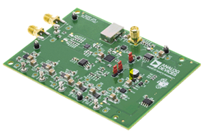
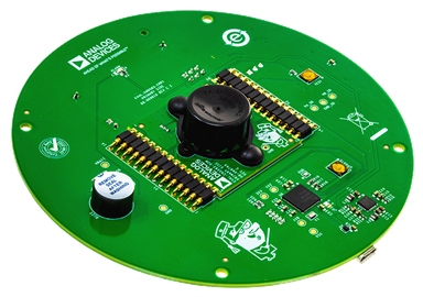
ADMV4828HB-EVALZ
Analog Devices Inc.The ADMV4828 is a silicon on insulator (SOI), 24.0 GHz to 29.5 GHz, mmW 5G beamformer. The RF integrated circuit (RFIC) is highly integrated and contains 16 independent transmit and receive channels. The ADMV4828 supports eight horizontal and eight vertical polarized antennas via independent RFV and RFH input/outputs.In transmit mode, both the RFV input and RFH input signals feed into separate amplifiers. Each path after the amplifiers splits into eight independent channels via the 1:8 power splitters. In receive mode, input signals pass through either the vertical or horizontal receive channels and combine via two independent 8:1 combiners to the common RFV pin or RFH pin. In either mode, each transmit and receive channel includes a vector modulator (VM) to control the phase, and two digital variable gain amplifiers (DVGAs) to control the amplitude. The VM provides a full 360? phase adjustment range in either transmit or receive mode to provide 6 bits of resolution for 5.625? phase steps. A phase step policy for the transmit and receive VM is provided to ensure optimum phase step performance. The total DVGA dynamic range in transmit mode is 34.5, which provides 6 bits of resolution that results in 0.5 dB amplitude steps and 5 bits of resolution that results in 1 dB amplitude steps. In receive mode, the total dynamic range is 28 dB, which provides 5 bits of resolution that results in 0.5 dB amplitude steps and 5 bits of resolution that results in 1 dB amplitude steps. The DVGAs provide a flat phase response across the full gain range. A gain policy for DVGA1 and DVGA2 is provided in the AN-2074 Application Note, ADMV4828 Application Note to ensure optimized performance across the attenuation range with 0.5 dB step resolution from 0 dB to 34.5 dB attenuation for transmit mode and 0.5 dB step resolution from 0 dB to 28 dB attenuation for receive mode. The transmit channels contain individual transmit power detectors to detect either modulated or continuous wave signals to calibrate for each channel gain as well as channel to channel gain mismatch. Each receive channel contains an RF power overload circuit (receive channel overload detection circuit) to prevent potential damage to the device as a result of blocker instances. The ADMV4828 RF ports can be connected directly to a patch antenna to create a dual polarization mmW 5G subarray.The ADMV4828 can be programmed using a 3-wire or 4-wire serial port interface (SPI). An integrated, on-chip low dropout (LDO) voltage regulator generates the 1.0 V supply for the SPI circuitry to reduce the number of supply domains required. Various SPI modes are available to enable fast startup and control during normal operation. The amplitude and phase for each channel can be set individually or multiple channels can be programmed simultaneously using the on-chip memory for beamforming. The on-chip memory can store up to 2048 beam positions that can be allocated for either transmit mode or receive mode for the horizontal channels and vertical channels. On-chip nonvolatile memory (NVM) is used to store the calibrated gain and phase offset coefficients and the reference values for each individual channel from the factory. These values are used to perform channel to channel or chip to chip calibration. In addition, four address pins (CHIP_ADDx) allow independent SPI control of up to 16 devices on the same serial lines. To control multiple devices via the same serial lines with the same instructions, activate broadcast mode via the external enable pin (BR_EN). Dedicated horizontal and vertical polarization load pins (LOAD_V and LOAD_H) provide the synchronization of all devices in the same array. A horizontal and vertical polarization transmit mode and receive mode control pin (TRX_H or TRX_V) is provided for fast switching between transmit mode and receive mode.The ADMV4828 comes in a compact, 304-ball, 10 mm ? 8.5 mm chip scale package ball grid array (CSP_BGA). The ADMV4828 operates over the ?40?C to +95?C case temperature (TC) range. This CSP_BGA package enables the ability to heatsink the ADMV4828 from the topside of the package for the most efficient thermal heatsinking and to allow flexible antenna placement on the opposite side of the printed circuit board (PCB).APPLICATIONSmmW 5G applicationBroadband communication
ADMV7320-EVALZ
Analog Devices Inc.The ADMV7320 is a fully integrated system in package (SiP),in phase/quadrature (I/Q) upconverter that operates betweenan intermediate frequency (IF) input range of dc and 2 GHzand a radio frequency (RF) output range of 81 GHz and 86 GHz.The device uses an image rejection mixer that is driven by a 6?local oscillator (LO) multiplier. The mixer RF output is followedby a variable gain amplifier (VGA) and a power amplifier (PA),providing a conversion gain of 33 dB typical. Differential I andQ mixer inputs are provided and can be driven with differentialI and Q baseband waveforms for direct conversion applications.Alternatively, the inputs can be driven using an external 90? hybridand two external 180 hybrids for single-ended applications.The ADMV7320 comes in a fully integrated, surface-mount,50-terminal, 16.00 mm ? 14.00 mm, chip array small outline nolead cavity (LGA_CAV) package. The ADMV7320 operatesover the ?40?C to +85?C temperature range.APPLICATIONS E-band communication systems High capacity wireless backhauls Test and measurement Aerospace and defense
ADN2830-EVALZ
Analog Devices Inc.The ADN2830 provides closed loop control of the average optical power of a continuous wave (CW) laser diode (LD) after initial factory setup. The control loop adjusts the laser IBIAS to maintain a constant Back Facet Monitor Photo Diode (MPD) current and hence a constant laser optical power. The external PSET resistor is adjusted during factory set up to set the desired optical power. RPSET is set at 1.23/IAV, where IAVis the MPD current corresponding to the desired optical power. Programmable alarms are provided for laser fail (end of life) and laser degrade (impending fail).The ADN2830 operates from a single power +5 V supply. It is available in 5mm ? 5mm LFCSP-32 Lead Frame Chip Scale.
ADN8831-EVALZ
Analog Devices Inc.The ADN88311 is a monolithic TEC controller. It has two integrated, zero drift, rail-to-rail comparators, and a PWM driver. A unique PWM driver works with an analog driver to control external selected MOSFETs in an H-bridge. By sensing the thermal detector feedback from the TEC, the ADN8831 can drive a TEC to settle the programmable temperature of a laser diode or a passive component attached to the TEC module.The ADN8831 supports NTC thermistors or positive temperature coefficient (PTC) RTDs. The target temperature is set as an analog voltage input either from a DAC or from an external resistor divider driven by a reference voltage source.A proportional integral differential (PID) compensation network helps to quickly and accurately stabilize the ADN8831 thermal control loop. An adjustable PID compensation network example is described in the AN-695 Application Note, Using the ADN8831TEC Controller Evaluation Board. A typical reference voltage of 2.5 V is available from the ADN8831 for thermistor temperature sensing or for TEC voltage/current measuring and limiting in both cooling and heating modes.Applications Thermoelectric cooler (TEC) temperature control DWDM optical transceiver modules Optical fiber amplifiers Optical networking systems Instruments requiring TEC temperature control1 Product is covered by U.S. Patent No. 6,486,643
ADN8833CB-EVALZ
Analog Devices Inc.The ADN8833 is a monolithic H-bridge TEC driver with integrat-ed 1 A power MOSFETs. It has a linear power stage with the linear driver (LDR) output and a pulse-width modulation (PWM) power stage with the SW output. Depending on the control voltage at the CONT input, the ADN8833 drives current through a TEC to settle the temperature of a laser diode or a passive component attached to the TEC module to the programmed target temperature.The control voltage applied to the CONT input is generated by a digital-to-analog converter (DAC) closing the digital proportional, integral, derivative (PID) loop of temperature control system.The internal 2.5 V reference voltage provides a 1% accurate output that is used to bias a voltage divider network to program the maximum TEC current and voltage limits for both the heating and cooling modes. It can also be a reference voltage for the DAC and the temperature sensing circuit, including a thermistor bridge and an analog-to-digital converter (ADC).APPLICATIONS TEC temperature control Optical modules Optical fiber amplifiers Optical networking systems Instruments requiring TEC temperature control
ADN8834CP-EVALZ
Analog Devices Inc.The ADN88341 is a monolithic TEC controller with an integrated TEC controller. It has a linear power stage, a pulse-width modulation (PWM) power stage, and two zero-drift, rail-to-rail operational amplifiers. The linear controller works with the PWM driver to control the internal power MOSFETs in an H-bridge configuration. By measuring the thermal sensor feedback voltage and using the integrated operational amplifiers as a proportional integral differential (PID) compensator to condition the signal, the ADN8834 drives current through a TEC to settle the temperature of a laser diode or a passive component attached to the TEC module to the programmed target temperature.The ADN8834 supports negative temperature coefficient (NTC) thermistors as well as positive temperature coefficient (PTC) resistive temperature detectors (RTD). The target temperature is set as an analog voltage input either from a digital-to-analog converter (DAC) or from an external resistor divider.The temperature control loop of the ADN8834 is stabilized by PID compensation utilizing the built in, zero drift chopper amplifiers. The internal 2.50 V reference voltage provides a 1% accurate output that is used to bias a thermistor temperature sensing bridge as well as a voltage divider network to program the maximum TEC current and voltage limits for both the heating and cooling modes. With the zero drift chopper amplifiers, extremely good long-term temperature stability is maintained via an autonomous analog temperature control loop.APPLICATIONS TEC temperature control Optical modules Optical fiber amplifiers Optical networking systems Instruments requiring TEC temperature control1 Product is covered by U.S. Patent No. 6,486,643.
ADN8834MB-EVALZ
Analog Devices Inc.The ADN88341 is a monolithic TEC controller with an integrated TEC controller. It has a linear power stage, a pulse-width modulation (PWM) power stage, and two zero-drift, rail-to-rail operational amplifiers. The linear controller works with the PWM driver to control the internal power MOSFETs in an H-bridge configuration. By measuring the thermal sensor feedback voltage and using the integrated operational amplifiers as a proportional integral differential (PID) compensator to condition the signal, the ADN8834 drives current through a TEC to settle the temperature of a laser diode or a passive component attached to the TEC module to the programmed target temperature.The ADN8834 supports negative temperature coefficient (NTC) thermistors as well as positive temperature coefficient (PTC) resistive temperature detectors (RTD). The target temperature is set as an analog voltage input either from a digital-to-analog converter (DAC) or from an external resistor divider.The temperature control loop of the ADN8834 is stabilized by PID compensation utilizing the built in, zero drift chopper amplifiers. The internal 2.50 V reference voltage provides a 1% accurate output that is used to bias a thermistor temperature sensing bridge as well as a voltage divider network to program the maximum TEC current and voltage limits for both the heating and cooling modes. With the zero drift chopper amplifiers, extremely good long-term temperature stability is maintained via an autonomous analog temperature control loop.APPLICATIONS TEC temperature control Optical modules Optical fiber amplifiers Optical networking systems Instruments requiring TEC temperature control1 Product is covered by U.S. Patent No. 6,486,643.
ADP1032CP-1-EVALZ
Analog Devices Inc.The ADP1032 is a high performance, isolated micropower management unit (PMU) that combines an isolated flyback and a dc-to-dc regulator providing two isolated power rails. Additionally, the ADP1032 contains four high speed serial peripheral interface (SPI) isolation channels and three general-purpose isolators for channel to channel applications where low power dissipation and small solution size is required. Operating over an input voltage range of 4.5 V to 60 V, the ADP1032 generates isolated output voltages of 6 V to 28 V (adjustable version) or 24 V (fixed version) for VOUT1, and factory programmable voltages of 5.15 V, 5.0 V, or 3.3 V for VOUT2.?By default, the ADP1032 flyback regulator operates at a 250 kHz switching frequency, and the buck regulator operates at 125 kHz.?The two regulators are phase shifted relative to each other to reduce electromagnetic interference (EMI). The ADP1032 can be driven by an external oscillator in the range of 350 kHz to 750 kHz to ease noise filtering in sensitive applications.?The digital isolators integrated in the ADP1032 use Analog Devices, Inc., iCoupler? chip scale transformer technology, optimized for low power and low radiated emissions. The ADP1032 is available in a 9 mm ? 7 mm, 41-lead LFCSP and is rated for a ?40?C to +125?C operating junction temperature range.?
ADP1032CP-4-EVALZ
Analog Devices Inc.The ADP1032 is a high performance, isolated micropower management unit (PMU) that combines an isolated flyback and a dc-to-dc regulator providing two isolated power rails. Additionally, the ADP1032 contains four high speed serial peripheral interface (SPI) isolation channels and three general-purpose isolators for channel to channel applications where low power dissipation and small solution size is required. Operating over an input voltage range of 4.5 V to 60 V, the ADP1032 generates isolated output voltages of 6 V to 28 V (adjustable version) or 24 V (fixed version) for VOUT1, and factory programmable voltages of 5.15 V, 5.0 V, or 3.3 V for VOUT2.?By default, the ADP1032 flyback regulator operates at a 250 kHz switching frequency, and the buck regulator operates at 125 kHz.?The two regulators are phase shifted relative to each other to reduce electromagnetic interference (EMI). The ADP1032 can be driven by an external oscillator in the range of 350 kHz to 750 kHz to ease noise filtering in sensitive applications.?The digital isolators integrated in the ADP1032 use Analog Devices, Inc., iCoupler? chip scale transformer technology, optimized for low power and low radiated emissions. The ADP1032 is available in a 9 mm ? 7 mm, 41-lead LFCSP and is rated for a ?40?C to +125?C operating junction temperature range.?
ADP1046A-100-EVALZ
Analog Devices Inc.The ADP1046A is a flexible, digital secondary side controller designed for ac-to-dc and isolated dc-to-dc secondary sideapplications. The ADP1046A is pin-compatible with theADP1043A and offers several enhancements and new features,including voltage feedforward and improved loop response to maximize efficiency.The ADP1046A is optimized for minimal component count,maximum flexibility, and minimum design time. Featuresinclude local and remote voltage sense, primary and secondary side current sense, digital pulse-width modulation (PWM)generation, current sharing, and redundant OrFET control. The control loop digital filter and compensation terms are integrated and can be programmed over the I2C interface. Programmableprotection features include overcurrent protection (OCP), over-voltage protection (OVP), undervoltage lockout (UVLO), and overtemperature protection (OTP).The built-in EEPROM provides extensive programming of theintegrated loop filter, PWM signal timing, inrush current, andsoft start timing and sequencing. Reliability is improved through a built-in checksum and programmable protection circuits.A comprehensive GUI is provided for easy design of loop filter characteristics and programming of the safety features.The industry-standard I2C bus provides access to the many monitoring and system test functions.The ADP1046A is available in a 32-lead LFCSP and operatesfrom a single 3.3 V supply.APPLICATIONS AC-to-DC power supplies Isolated dc-to-dc power supplies Redundant power supply systems Server, storage, network, and communications infrastructure
ADP1046ADC1-EVALZ
Analog Devices Inc.The ADP1046A is a flexible, digital secondary side controller designed for ac-to-dc and isolated dc-to-dc secondary sideapplications. The ADP1046A is pin-compatible with theADP1043A and offers several enhancements and new features,including voltage feedforward and improved loop response to maximize efficiency.The ADP1046A is optimized for minimal component count,maximum flexibility, and minimum design time. Featuresinclude local and remote voltage sense, primary and secondary side current sense, digital pulse-width modulation (PWM)generation, current sharing, and redundant OrFET control. The control loop digital filter and compensation terms are integrated and can be programmed over the I2C interface. Programmableprotection features include overcurrent protection (OCP), over-voltage protection (OVP), undervoltage lockout (UVLO), and overtemperature protection (OTP).The built-in EEPROM provides extensive programming of theintegrated loop filter, PWM signal timing, inrush current, andsoft start timing and sequencing. Reliability is improved through a built-in checksum and programmable protection circuits.A comprehensive GUI is provided for easy design of loop filter characteristics and programming of the safety features.The industry-standard I2C bus provides access to the many monitoring and system test functions.The ADP1046A is available in a 32-lead LFCSP and operatesfrom a single 3.3 V supply.APPLICATIONS AC-to-DC power supplies Isolated dc-to-dc power supplies Redundant power supply systems Server, storage, network, and communications infrastructure
ADP1055-EVALZ
Analog Devices Inc.The ADP1055 is a flexible, feature-rich digital secondary side controller that targets ac-to-dc and isolated dc-to-dc secondary side applications. The ADP1055 is optimized for minimal component count, maximum flexibility, and minimum design time. Features include differential remote voltage sense, primary and secondary side current sense, pulse-width modulation (PWM) generation, frequency synchronization, redundant OVP, and current sharing. The control loop digital filter and compensation terms are integrated and can be programmed over the PMBus? interface. Programmable protection features include overcurrent (OCP), overvoltage (OVP) limiting, undervoltage lockout (UVLO), and external overtemperature (OTP).The built-in EEPROM provides extensive programming of the integrated loop filter, PWM signal timing, inrush current, and soft start timing and sequencing. Reliability is improved through a built-in checksum and programmable protection circuits.A comprehensive GUI is provided for easy design of loop filter characteristics and programming of the safety features. The industry-standard PMBus provides access to the many monitoring and system test functions. The ADP1055 is available in a 32-lead LFCSP and operates from a single 3.3 V supply.APPLICATIONS Isolated dc-to-dc power supplies and modules Redundant power supply systems
ADP121CB-1.8-EVALZ
Analog Devices Inc.The ADP121 is a quiescent current, low dropout, linear regulator that operates from 2.3 V to 5.5 V and provides up to 150 mA of output current. The low 135 mV dropout voltage at 150 mA load improves efficiency and allows operation over a wide input voltage range. The low 30 ?A of quiescent current at full load makes the ADP121 ideal for battery-operated portable equipment.The ADP121 is available in output voltages ranging from 1.2 V to 3.3 V. The parts are optimized for stable operation with small 1 ?F ceramic output capacitors. The ADP121 delivers good transient performance with minimal board area.Short-circuit protection and thermal overload protection circuits prevent damage in adverse conditions. The ADP121 is available in a tiny 5-lead TSOT and 4-ball 0.4 mm pitch WLCSP pack-ages and utilizes the smallest footprint solution to meet a variety of portable applications.
ADP121UJZ-REDYKIT
Analog Devices Inc.The ADP121 is a quiescent current, low dropout, linear regulator that operates from 2.3 V to 5.5 V and provides up to 150 mA of output current. The low 135 mV dropout voltage at 150 mA load improves efficiency and allows operation over a wide input voltage range. The low 30 ?A of quiescent current at full load makes the ADP121 ideal for battery-operated portable equipment.The ADP121 is available in output voltages ranging from 1.2 V to 3.3 V. The parts are optimized for stable operation with small 1 ?F ceramic output capacitors. The ADP121 delivers good transient performance with minimal board area.Short-circuit protection and thermal overload protection circuits prevent damage in adverse conditions. The ADP121 is available in a tiny 5-lead TSOT and 4-ball 0.4 mm pitch WLCSP pack-ages and utilizes the smallest footprint solution to meet a variety of portable applications.
ADP150CB-3.3-EVALZ
Analog Devices Inc.The ADP150 is an ultralow noise (9 ?V), low dropout, linear regulator that operates from 2.2 V to 5.5 V and provides up to 150 mA of output current. The low 105 mV dropout voltage at 150 mA load improves efficiency and allows operation over a wide input voltage range.Using an innovative circuit topology, the ADP150 achieves ultralow noise performance without the necessity of an additional noise bypass capacitor, making it ideal for noise sensitive analog and RF applications. The ADP150 also achieves ultralow noise performance without compromising PSRR or line and load transient performance. The ADP150 offers the best combination of ultralow noise and quiescent current consumption to maximize battery life in portable applications.The ADP150 is specifically designed for stable operation with tiny 1 ?F ? 30% ceramic input and output capacitors to meet the requirements of high performance, space-constrained applications.The ADP150 is available in 14 fixed output voltage options, ranging from 1.8 V to 3.3 V.Short-circuit and thermal overload protection circuits prevent damage in adverse conditions. The ADP150 is available in tiny 5-lead TSOT and 4-ball, 0.4 mm pitch WLCSP packages for the smallest footprint solution to meet a variety of portable power applications.Applications Mobile phones Digital camera and audio devices Portable and battery-powered equipment Post dc-to-dc regulation Portable medical devices RF, PLL, VCO, and clock power supplies
ADP150UJZ-REDYKIT
Analog Devices Inc.The ADP150 is an ultralow noise (9 ?V), low dropout, linear regulator that operates from 2.2 V to 5.5 V and provides up to 150 mA of output current. The low 105 mV dropout voltage at 150 mA load improves efficiency and allows operation over a wide input voltage range.Using an innovative circuit topology, the ADP150 achieves ultralow noise performance without the necessity of an additional noise bypass capacitor, making it ideal for noise sensitive analog and RF applications. The ADP150 also achieves ultralow noise performance without compromising PSRR or line and load transient performance. The ADP150 offers the best combination of ultralow noise and quiescent current consumption to maximize battery life in portable applications.The ADP150 is specifically designed for stable operation with tiny 1 ?F ? 30% ceramic input and output capacitors to meet the requirements of high performance, space-constrained applications.The ADP150 is available in 14 fixed output voltage options, ranging from 1.8 V to 3.3 V.Short-circuit and thermal overload protection circuits prevent damage in adverse conditions. The ADP150 is available in tiny 5-lead TSOT and 4-ball, 0.4 mm pitch WLCSP packages for the smallest footprint solution to meet a variety of portable power applications.Applications Mobile phones Digital camera and audio devices Portable and battery-powered equipment Post dc-to-dc regulation Portable medical devices RF, PLL, VCO, and clock power supplies
ADP151CPZ-REDYKIT
Analog Devices Inc.The ADP151 is an ultralow noise, low dropout (LDO) linear regulator that operates from 2.2 V to 5.5 V and provides up to 200 mA of output current. The low 135 mV dropout voltage at 200 mA load improves efficiency and allows operation over a wide input voltage range.Using an innovative circuit topology, the ADP151 achieves ultralow noise performance without the necessity of a bypass capacitor, making the device ideal for noise-sensitive analog and RF applications. The ADP151 also achieves ultralow noise performance without compromising the power supply rejection ratio (PSRR) or transient line and load performance. The low 265 ?A of operating supply current at 200 mA load makes the ADP151 suitable for battery-operated portable equipment.The ADP151 also includes an internal pull-down resistor on the EN input.The ADP151 is specifically designed for stable operation with tiny 1 ?F, ?30% ceramic input and output capacitors to meet the requirements of high performance, space constrained applications.The ADP151 is capable of 16 fixed output voltage options, ranging from 1.1 V to 3.3 V.Short-circuit and thermal overload protection circuits prevent damage in adverse conditions. The ADP151 is available in tiny 5-lead TSOT, 6-lead LFCSP, and 4-ball, 0.4 mm pitch, halide-free WLCSP packages for the smallest footprint solution to meet a variety of portable power application requirements.APPLICATIONS RF, voltage controlled oscillator (VCO), and phase locked loop (PLL) power supplies Mobile phones Digital camera and audio devices Portable and battery-powered equipment Post dc-to-dc regulation Portable medical devices Automotive
ADP1607-001-EVALZ
Analog Devices Inc.The ADP1607 is a high efficiency, synchronous, fixed frequency, step-up dc-to-dc switching converter with an adjustable output voltage between 1.8 V and 3.3 V for use in portable applications.The 2 MHz operating frequency enables the use of small footprint, low profile external components. Additionally, the synchronous rectification, internal compensation, internal fixed current limit, and current mode architecture allow for excellent transient response and a minimal external part count.Other key features include fixed PWM and light load PFM mode options, true output isolation, thermal shutdown (TSD), and logic controlled enable. Available in a lead-free, thin, 6-lead LFCSP package, the ADP1607 is ideal for providing efficient power conversion in portable devices.APPLICATIONS 1-cell and 2-cell alkaline and NiMH/NiCd powered devices Portable audio players, instruments, and medical devices Solar cell applications Miniature hard disk power supplies Power LED status indicators
ADP160UJZ-REDYKIT
Analog Devices Inc.The ADP160 / ADP161 / ADP162 / ADP163?are ultralow quiescentcurrent, low dropout, linear regulators that operate from 2.2 Vto 5.5 V and provide up to 150 mA of output current. The low195 mV dropout voltage at 150 mA load improves efficiency andallows operation over a wide input voltage range.The ADP16x are specifically designed for stable operation withtiny 1 ?F ? 30% ceramic input and output capacitors to meetthe requirements of high performance, space-constrainedapplications.The ADP160 is available in 15 fixed output voltage options,ranging from 1.2 V to 4.2 V. The ADP160 / ADP161 also includea switched resistor to discharge the output automatically when the LDO is disabled. The ADP162 is identical to the ADP160but does not include the output discharge function.The ADP161and ADP163 are available as a adjustable outputvoltage regulators. They are only available in a 5-lead TSOTpackage. The ADP163 is identical to the ADP161 but does notinclude the output discharge function.Short-circuit and thermal overload protection circuits preventdamage in adverse conditions. The ADP160 and ADP162 areavailable in a tiny 5-lead TSOT and a 4-ball, 0.5 mm pitchWLCSP package for the smallest footprint solution to meet avariety of portable power applications.APPLICATIONS Mobile phones Digital cameras and audio devices Portable and battery-powered equipment Post dc-to-dc regulation Portable medical devices
ADP1610-EVALZ
Analog Devices Inc.The ADP1610 is a dc-to-dc step-up switching converter with an integrated 1.2 A, 0.2 ? power switch capable of providing an output voltage as high as 12 V. With a package height of less that 1.1 mm, the ADP1610 is optimal for space-constrained applications such as portable devices or thin film transistor (TFT) liquid crystal displays (LCDs). The ADP1610 operates in pulse-width modulation (PWM) current mode with up to 92% efficiency. Adjustable soft start prevents inrush currents at startup. The pin-selectable switching frequency and PWM current-mode architecture allow excellent transient response, easy noise filtering, and the use of small, cost-saving external inductors and capacitors. The ADP1610 is offered in the Pb-free 8-lead MSOP and operates over the temperature range of ?40?C to +85?C.APPLICATIONS TFT LC bias supplies Portable applications Industrial/instrumentation equipment


