
LT3958EUHE Boost Demo Board | 11V-40VIN; VOUT = 48V @ 0.5A
Analog Devices Inc.Demonstration circuit 1569A is a High Voltage Monolithic Boost Converter featuring the LT3958. The LT3958 can be configured as a boost, flyback, SEPIC, and inverting converter, but the demonstration circuit is assembled as a boost. The input voltage range is 11V to 40V and the output voltage is 48V with 500mA over the entire input voltage range. The LT3958 has an internal n-channel 3.3A, 84V power switch for high voltage, power, and efficiency. The dual paddle package provides excellent heat dissipation for the internal power switch. The LT3958 current-mode dc/dc converter features adjustable switching frequency, soft-start, compensation, shutdown and undervoltage lockout with hysteresis, and a feedback pin (FBX) that can be used in both positive and negative applications. A SYNC input can be used to synchronize the switching at a frequency higher than the IC is programmed.

DC1572A
Analog Devices Inc.The LTC3615/LTC3615-1 are dual 3A synchronous stepdown regulators using a current mode, constant-frequency architecture. The DC supply current is only 130?A (Burst Mode operation at no-load) while maintaining the output voltages, dropping to zero current in shutdown. The 2.25V to 5.5V input supply range makes the parts ideally suited for single Li-Ion applications. 100% duty cycle capability provides low dropout operation, which extends operating time in battery-operated systems.The operating frequency is externally programmable up to 4MHz, allowing the use of small surface mount inductors. 0?, 90?, or 180? (LTC3615) or 140?/180? (LTC3615-1) of phase shift between the two channels can be selected to minimize input current ripple and output voltage ripple in a dual 3A or single 6A output configuration. Programmable slew rate limiting reduces EMI, and external synchronization can be applied up to 4MHz.The internal synchronous switches increase efficiency and eliminate the need for external catch diodes, saving external components and board space.The LTC3615/LTC3615-1 are offered in leadless 24-pin 4mm ? 4mm QFN and thermally enhanced 24-pin eTSSOP packages.Applications Point-of-Load Supplies Distributed Power Supplies Portable Computer Systems DDR Memory Termination Handheld Devices

DC1574A
Analog Devices Inc.The LTC3612 is a low quiescent current monolithic synchronous buck regulator using a current mode, constant frequency architecture. The no-load DC supply current in sleep mode is only 70?A while maintaining the output voltage (Burst Mode operation) at no load, dropping to zero current in shutdown. The 2.25V to 5.5V input supply voltage range makes the LTC3612 ideally suited for single Li-Ion as well as fixed low voltage input applications. 100% duty cycle capability provides low dropout operation, extending the operating time in battery-powered systems.The operating frequency is externally programmable up to 4MHz, allowing the use of small surface mount inductors. For switching noise-sensitive applications, the LTC3612 can be synchronized to an external clock at up to 4MHz.Forced continuous mode operation in the LTC3612 reduces noise and RF interference. Adjustable compensation allows the transient response to be optimized over a wide range of loads and output capacitors.The internal synchronous switch increases efficiency and eliminates the need for an external catch diode, saving external components and board space. The LTC3612 is offered in a leadless 20-pin 3mm ? 4mm QFN or a thermally enhanced 20-pin TSSOP package.APPLICATIONS Point-of-Load Supplies Distributed Power Supplies Portable Computer Systems DDR Memory Termination Handheld Devices

LTC3108EDE Demo Board | Ultralow Voltage Step-Up Converter and Power Manager
Analog Devices Inc.DC1582B-A: Demo Board for the LTC3108 Ultralow Voltage Step-Up Converter and Power Manager.

LTC4070EDDB Demo Board | Simple Low-IQ Battery Charger/Protector with NTC Thermistor Input
Analog Devices Inc.DC1584A: Demo Board for the LTC4070 Li-Ion/Polymer Shunt Battery Charger System.

LTC2635-HMI12 | 12-Bit Quad I2C DAC (4.096V Internal Reference Mode, Reset to Mid-Scale), Requires DC590
Analog Devices Inc.DC1593A-D: Demo Board for LTC2635-12 Quad 12-Bit I2C VOUT DACs with 10ppm/°C Reference.

DC1595A
Analog Devices Inc.The LT3799 is an isolated flyback controller with power factor correction specifically designed for driving LEDs. The controller operates using critical conduction mode allowing the use of a small transformer. Using a novel current sensing scheme, the controller is able to deliver a well regulated current to the secondary side without using an opto-coupler. A strong gate driver is included to drive an external high voltage MOSFET. Utilizing an onboard multiplier, the LT3799 typically achieves power factors of 0.97. The FAULT pin provides notification of open and short LED conditions.The LT3799 uses a micropower hysteretic start-up to efficiently operate at offline input voltages, with a third winding to provide power to the part. An internal LDO provides a well regulated supply for the part?s internal circuitry and gate driver. TRIAC Dimmable LED Current Regulation LT3799 YES ?10% LT3799-1 NO ?5% Applications Offline 4W to 100W+ LED Applications High DC VIN LED Applications

LTC3855EFE Demo Board | Dual Output VIN = 13V to 36V, VOUT1 = 12V @ 6A, VOUT2 = 5V @ 10A
Analog Devices Inc.Demonstration circuit DC1617A is a dual output synchronous buck converter featuring the LTC3855EFE in a high density, two sided drop-in layout with power components on the top and the control circuit on the bottom. The package style for the LTC3855EFE is a 38-lead TSSOP. The board comes in two assembly types. The –B assembly is a high power, 12V/6A and 5V/10A converter with a 13V to 36V input. A sense resistor is used to provide a precise current limit. Unlike the –A assembly, on the –B assembly the remote sense diff amp is bypassed since VOUT2 is > 3.3V.

LT3845AEFE Demo Board | 16V ≤ VIN ≤ 60V, VOUT = 12V @ 10A
Analog Devices Inc.Demonstration Circuit 1619A is a 100kHz to 500kHz programmable frequency, high voltage, current mode DC/DC step-down converter featuring the LT3845A. The operating frequency can be synchronized up to 600kHz. This demo board is designed for 12V output at up to 10A (120W) from a 16V to 60V input.
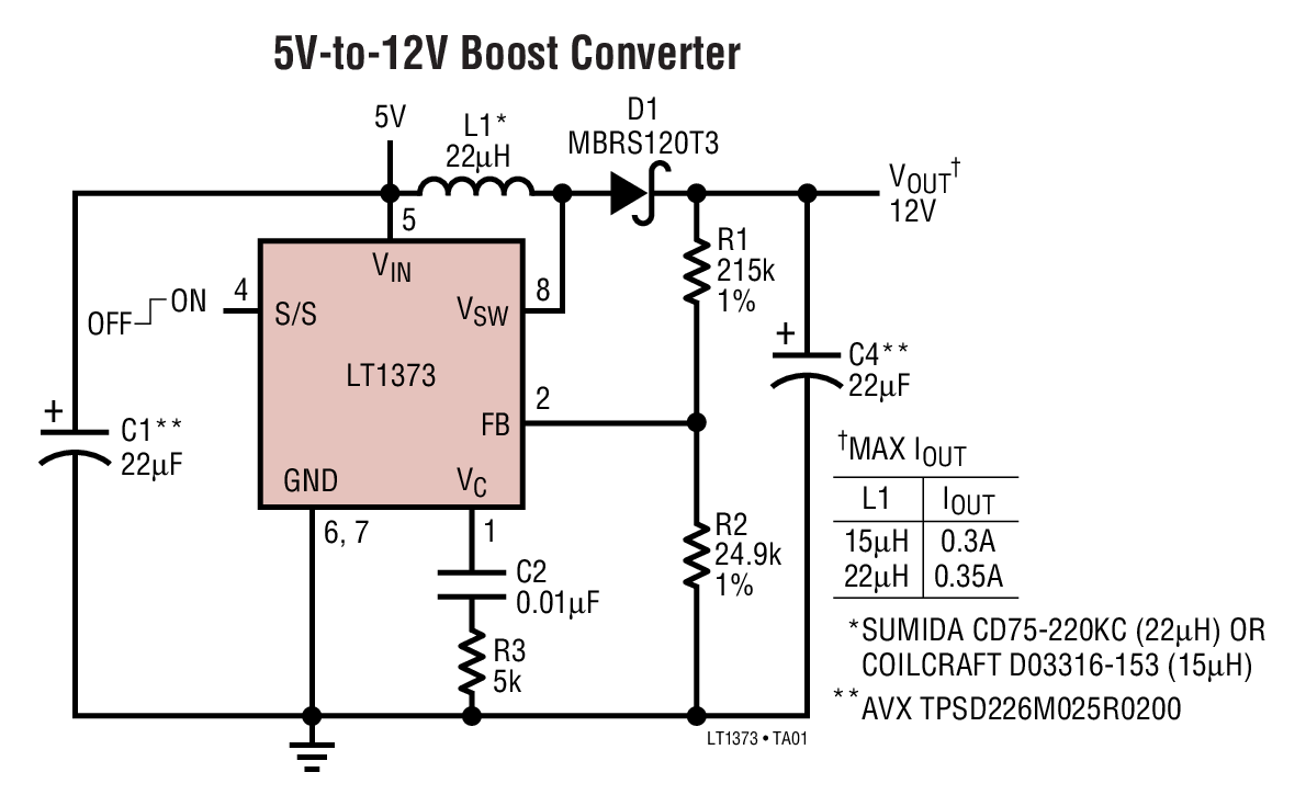
DC161A
Analog Devices Inc.The LT1373 is a low supply current high frequency current mode switching regulator. It can be operated in all standard switching configurations including boost, buck, flyback, forward, inverting and ?Cuk.? A 1.5A high efficiency switch is included on the die, along with all oscillator, control and protection circuitry. All functions of the LT1373 are integrated into 8-pin SO/PDIP packages.Compared to the 500kHz LT1372, which draws 4mA of quiescent current, the LT1373 switches at 250kHz, typically consumes only 1mA and has higher efficiency. High frequency switching allows for small inductors to be used. All surface mount components consume less than 0.6 square inch of board space.New design techniques increase flexibility and maintain ease of use. Switching is easily synchronized to an external logic level source. A logic low on the shutdown pin reduces supply current to 12?A. Unique error amplifier circuitry can regulate positive or negative output voltage while maintaining simple frequency compensation techniques. Nonlinear error amplifier transconductance reduces output overshoot on start-up or overload recovery. Oscillator frequency shifting protects external components during overload conditions.Applications Boost Regulators CCFL Backlight Driver Laptop Computer Supplies Multiple Output Flyback Supplies Inverting Supplies

DC1620A-C
Analog Devices Inc.The LTC2185/LTC2184/LTC2183 are two-channel simultaneous sampling 16-bit A/D converters designed for digitizing high frequency, wide dynamic range signals. They are perfect for demanding communications applications with AC performance that includes 76.8dB SNR and 90dB spurious free dynamic range (SFDR). Ultralow jitter of 0.07psRMS allows undersampling of IF frequencies with excellent noise performance. DC specs include ?2LSB INL (typ), ?0.5LSB DNL (typ) and no missing codes over temperature. The transition noise is 3.4LSBRMS. The digital outputs can be either full rate CMOS, Double Data Rate CMOS, or Double Data Rate LVDS. A separate output power supply allows the CMOS output swing to range from 1.2V to 1.8V. The ENC+ and ENC? inputs may be driven differentially or single-ended with a sine wave, PECL, LVDS, TTL, or CMOS inputs. An optional clock duty cycle stabilizer allows high performance at full speed for a wide range of clock duty cycles.Applications Communications Cellular Base Stations Software Defined Radios Portable Medical Imaging Multi-Channel Data Acquisition Nondestructive Testing

DC1620A-E
Analog Devices Inc.The LTC2182/LTC2181/LTC2180 are two-channel simultaneous sampling 16-bit A/D converters designed for digitizing high frequency, wide dynamic range signals. They are perfect for demanding communications applications with AC performance that includes 77dB SNR and 90dB spurious free dynamic range (SFDR). Ultralow jitter of 0.07psRMS allows undersampling of IF frequencies with excellent noise performance. DC specs include ?2LSB INL (typ), ?0.5LSB DNL (typ) and no missing codes over temperature. The transition noise is 3.3LSBRMS. The digital outputs can be either full rate CMOS, Double Data Rate CMOS, or Double Data Rate LVDS. A separate output power supply allows the CMOS output swing to range from 1.2V to 1.8V. The ENC+ and ENC? inputs may be driven differentially or single-ended with a sine wave, PECL, LVDS, TTL, or CMOS inputs. An optional clock duty cycle stabilizer allows high performance at full speed for a wide range of clock duty cycles.Applications Communications Cellular Base Stations Software Defined Radios Portable Medical Imaging Multi-Channel Data Acquisition Nondestructive Testing
DC1620A-F
Analog Devices Inc.The LTC2182/LTC2181/LTC2180 are two-channel simultaneous sampling 16-bit A/D converters designed for digitizing high frequency, wide dynamic range signals. They are perfect for demanding communications applications with AC performance that includes 77dB SNR and 90dB spurious free dynamic range (SFDR). Ultralow jitter of 0.07psRMS allows undersampling of IF frequencies with excellent noise performance. DC specs include ?2LSB INL (typ), ?0.5LSB DNL (typ) and no missing codes over temperature. The transition noise is 3.3LSBRMS. The digital outputs can be either full rate CMOS, Double Data Rate CMOS, or Double Data Rate LVDS. A separate output power supply allows the CMOS output swing to range from 1.2V to 1.8V. The ENC+ and ENC? inputs may be driven differentially or single-ended with a sine wave, PECL, LVDS, TTL, or CMOS inputs. An optional clock duty cycle stabilizer allows high performance at full speed for a wide range of clock duty cycles.Applications Communications Cellular Base Stations Software Defined Radios Portable Medical Imaging Multi-Channel Data Acquisition Nondestructive Testing

LTC2145-14: 14-bit 125Msps ADC, DDR LVDS Outputs, 5-140MHz, Requires DC890, LVDS_XFMR and DC1075
Analog Devices Inc.DC1620A-G: Demo Board for LTC2145-14 14-Bit, 125Msps Low Power Dual ADCs.

LTC4227CUFD-3 Demo Board: Dual Ideal Diode and Single Hot Swap Controller with Fault Latch-Off and 1.6ms On Delay
Analog Devices Inc.Demonstration circuit 1625A is intended to demonstrate performance of the LTC4227-1/LTC4227-2/LTC4227-3/LTC4227-4 dual ideal diode and Hot Swap™ controller. Each rail has an individual ideal diode. Ideal diode outputs are connected to the load through a single Hot Swap circuit.

LTC4226CUD-1 Demo Board: Dual Hot Swap Controller with Latch Off
Analog Devices Inc.DC1627A-A: Demo Board for the LTC4226 Wide Operating Range Dual Hot Swap Controller.

LTC2472, Selectable 208sps/833sps, 16-Bit ΔΣ ADCs with 10ppm/°C Max Precision Reference. (Requires DC590B)
Analog Devices Inc.DC1629A: Demo Board for the LTC2472 Selectable 208sps/833sps, 16-Bit ΔΣ ADCs with 10ppm/°C Max Precision Reference.

LTC5587IDD | 6GHz RMS Power Detector with Digital Output Demo Board (RF=1.75 to 2.2GHz) - Companion Serial Interface board DC590B may be ordered separately.
Analog Devices Inc.DC1638A: Demo Board for LTC5587 6 GHz RMS Power Detector with Digital Output.

LTM8061-4.1 Demo Board | 6.5V ≤ VIN ≤ 32V, 2A µModule Buck Li-Ion Battery Charger, VOUT = 4.1V @ 2A
Analog Devices Inc.Demonstration circuits 1645A-A, 1645A-B, 1645A-C and 1645A-D feature the LTM8061, a 32V, 2A μModule® Li-Ion battery charger. Operating from a 6.5V to 32V input source, the 1645A-A and 1645A-B demo circuits charge single cell Li-Ion batteries to float voltages of 4.1V or 4.2V respectively. The 1645A-C and 1645A-D demo circuits operate from a 12V to 32V input source, and charge dual cell Li-Ion battery packs to float voltages of 8.2V or 8.4V. JP1 turns the converter on or off. JP2 allows for easy selection of C/10 or timer charge termination.

LTC3388EMSE-3 Demo Board | 2.8V ≤ VIN ≤ 20V, VOUT = 2.8V to 5V @ 50mA
Analog Devices Inc.Demonstration Circuit DC1658A is a 20V High Efficiency Nanopower Step-Down Regulator featuring the LTC3388-1/ LTC3388-3. The LTC3388 is an ultralow quiescent current power supply designed to regulate the output voltage by means of a nanopower high efficiency synchronous buck regulator. The input current is only 720nA typical at no load while maintaining output voltage regulation, capable of supplying 50mA of load current. The LTC3388-1/ LTC3388-3 also in-corporates an accurate undervoltage lockout feature to disable the converter and maintain a low quiescent current state when the input voltage falls below 2.3V. In regulation, the LTC3388-1/LTC3388-3 enter a sleep state in which both input and output quiescent currents are minimal. The buck converter turns on and off as needed to maintain regulation. An additional standby mode disables the buck switching while the output is in regulation for short duration loads requiring low ripple.


