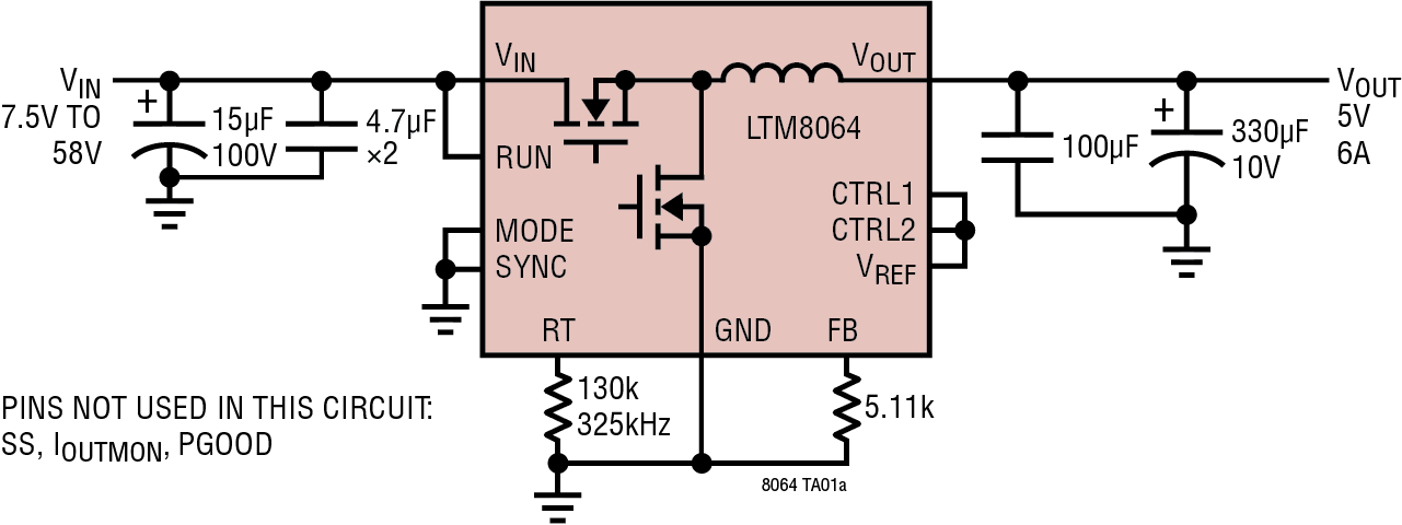
DC2237A
Analog Devices Inc.The LTM8064 is a 58VIN, 6A, constant-voltage, constantcurrent (CVCC), step-down ?Module? (power module) regulator. Included in the package are the switching controller, power switches, inductor and support components. Operating over an input voltage range of 6V to 58V, the LTM8064 supports an output voltage range of 1.2V to 36V. CVCC operation allows the LTM8064 to accurately regulate its output current up to 7A when sourcing and 9.1A when sinking over the entire output range. The output current can be set by a control voltage, a single resistor or a thermistor. To set the switching frequency, simply place a resistor from the RT pin to ground. A resistor from FB to ground will set the output voltage. Only the bulk input and output filter capacitors are needed to finish the design.The LTM8064 is packaged in a thermally enhanced, compact (16mm ? 11.9mm ? 4.92mm) over-molded ball grid array (BGA) package suitable for automated assembly by standard surface mount equipment. The LTM8064 is RoHS compliant.Applications Short- Circuit Protection or Accurate Output Current?Limit High Power LED Drive Peltier Driver Motor Drive Battery/Supercap Charging and Cell Balancing

DC2243A
Analog Devices Inc.The LT3668 is a monolithic triple power supply composed of a 400mA buck switching regulator and two 200mA low dropout linear tracking regulators (LDOs).This provides a complete and robust power solution for applications that require the power supply of a sensor to tightly track the power supply of a measurement ASIC.Each tracking LDO supplies 200mA of output current with a typical dropout voltage of 340mV, and each LDO has an accurate resistor programmable current limit.Internal protection circuitry includes reverse-battery protection, current limiting, thermal limiting and reverse current protection.The buck regulator includes a high efficiency switch, a boost diode, and the necessary oscillator, control and logic circuitry. Current mode topology is used for fast transient response and good loop stability. Low ripple Burst Mode operation maintains high efficiency at low output currents while keeping output ripple below 15mV in a typical application.The LT3668 is available in a thermally-enhanced 16-lead MSOP package with exposed pad for low thermal resistance.Applications Fault-Protected Sensor Supply Automotive and Industrial Supplies Power for Portable Instrumentation

DC2246B
Analog Devices Inc.The LT3042 is a high performance low dropout linear regulator featuring LTC?s ultralow noise and ultrahigh PSRR architecture for powering noise sensitive RF applications. Designed as a precision current reference followed by a high performance voltage buffer, the LT3042 can be easily paralleled to further reduce noise, increase output current and spread heat on the PCB.The device supplies 200mA at a typical 350mV dropout voltage. Operating quiescent current is nominally 2mA and drops to

DC2248A-A
Analog Devices Inc.The LTC6951 is a high performance, low noise, Phase Locked Loop (PLL) with a fully integrated VCO. The low noise VCO uses no external components and is internally calibrated to the correct output frequency with no external system support.The clock generation section provides five outputs based on the VCO prescaler signal with individual dividers for each output. Four outputs feature very low noise, low skew CML logic. The fifth output is low noise LVDS. All outputs can be synchronized and set to precise phase alignment using the programmable delays.Choose the LTC6951-1 if any desired output frequency falls in the ranges 2.5GHz to 2.7GHz, 1.66GHz to 1.8GHz, or 1.25GHz to 1.35GHz. Choose the LTC6951 for all other frequencies.Applications High Performance Data Converter Clocking Wireless Infrastructure Test and Measurement
DC2248A-B
Analog Devices Inc.The LTC6951 is a high performance, low noise, Phase Locked Loop (PLL) with a fully integrated VCO. The low noise VCO uses no external components and is internally calibrated to the correct output frequency with no external system support.The clock generation section provides five outputs based on the VCO prescaler signal with individual dividers for each output. Four outputs feature very low noise, low skew CML logic. The fifth output is low noise LVDS. All outputs can be synchronized and set to precise phase alignment using the programmable delays.Choose the LTC6951-1 if any desired output frequency falls in the ranges 2.5GHz to 2.7GHz, 1.66GHz to 1.8GHz, or 1.25GHz to 1.35GHz. Choose the LTC6951 for all other frequencies.Applications High Performance Data Converter Clocking Wireless Infrastructure Test and Measurement

DC2254A-A
Analog Devices Inc.The LTC2956 is a micropower, wide input voltage range, configurable wake-up timer with pushbutton control. It periodically wakes up and turns on a connected system to perform tasks like monitoring temperature or capturing images. After completing the task, the LTC2956 turns the system off to conserve power.The wake-up timer period can be adjusted from 250ms to 39 days using configuration resistors. The system awake time can be controlled by the input pulse at the SLEEP pin or adjusted by the capacitor at the ONMAX pin. The LTC2956 operates over a wide supply input range from 1.5V to 36V. The low 800nA quiescent current suits battery powered applications.The pushbutton input allows the user to shutdown, turn on or reset the wake-up timer. With the timer in shutdown, the quiescent current drops to 300nA. The LTC2956 also provides three status outputs to indicate mode transitions and pushbutton events. Two versions are available for applications requiring either positive or negative enable polarities.Applications Heartbeat Timers Periodic Wake-Up Control Portable and Battery-Powered Equipment Intervalometers Data Acquisition

DC2259A
Analog Devices Inc.The LTC6811 is a multicell battery stack monitor that measures up to 12 series connected battery cells with a total measurement error of less than 1.2mV. The cell measurement range of 0V to 5V makes the LTC6811 suitable for most battery chemistries. All 12 cells can be measured in 290?s, and lower data acquisition rates can be selected for high noise reduction.Multiple LTC6811 devices can be connected in series, permitting simultaneous cell monitoring of long, high voltage battery strings. Each LTC6811 has an isoSPI interface for high speed, RF-immune, long distance communications. Using the LTC6811-1, multiple devices are connected in a daisy chain with one host processor connection for all devices. Using the LTC6811-2, multiple devices are connected in parallel to the host processor, with each device individually addressed.The LTC6811 can be powered directly from the battery stack or from an isolated supply. The LTC6811 includes passive balancing for each cell, with individual PWM duty cycle control for each cell. Other features include an onboard 5V regulator, five general purpose I/O lines and a sleep mode, where current consumption is reduced to 4?A.Applications Electric and Hybrid Electric Vehicles Backup Battery Systems Grid Energy Storage High Power Portable Equipment
DC2260A
Analog Devices Inc.The LTC6811 is a multicell battery stack monitor that measures up to 12 series connected battery cells with a total measurement error of less than 1.2mV. The cell measurement range of 0V to 5V makes the LTC6811 suitable for most battery chemistries. All 12 cells can be measured in 290?s, and lower data acquisition rates can be selected for high noise reduction.Multiple LTC6811 devices can be connected in series, permitting simultaneous cell monitoring of long, high voltage battery strings. Each LTC6811 has an isoSPI interface for high speed, RF-immune, long distance communications. Using the LTC6811-1, multiple devices are connected in a daisy chain with one host processor connection for all devices. Using the LTC6811-2, multiple devices are connected in parallel to the host processor, with each device individually addressed.The LTC6811 can be powered directly from the battery stack or from an isolated supply. The LTC6811 includes passive balancing for each cell, with individual PWM duty cycle control for each cell. Other features include an onboard 5V regulator, five general purpose I/O lines and a sleep mode, where current consumption is reduced to 4?A.Applications Electric and Hybrid Electric Vehicles Backup Battery Systems Grid Energy Storage High Power Portable Equipment

DC2268A-E
Analog Devices Inc.The LTM4630-1A/LTM4630-1B are dual 18A or single 36A output step-down ?Module? (power module) regulators with ?0.8% (LTM4630-1A) and ?1.5% (LTM4630-1B) total DC output error, respectively, with ?3% transient output error. Included in the package are the switching controller, power FETs, inductors, and all supporting components. External compensation allows for fast transient response to minimize output capacitance when powering FPGAs, ASICs, and processors. With synchronized multiphase parallel current sharing, four LTM4630-1 devices can deliver up to 144A. The LTM4630-1 is offered in a 16mm ? 16mm ? 5.01 BGA package. Features Vout LTM4630 ? 0.6V to 1.8V LTM4630-1 0.8% DC and 3% Transient Accuracy 0.6V to 1.8V LTM4630A Higher Light Load Efficiency 0.6V to 5.3V Applications FPGA, ASIC, ?Processor Core Voltage Regulation Information, Communication Systems

LTM4650-1 Dual 25A or Single 50A µModule Regulator
Analog Devices Inc.Demonstration circuit 2268A-H is a high efficiency, high density, dual 25A, switch mode step-down power supply on a compact 1.5-inch × 1.2-inch PCB. It features the LTM4650-1 µModule® regulator. The input voltage is from 4.5V to 15V. The output voltage is programmable from 0.6V to 1.8V. DC2268A-H can deliver up to 25A maximum in each channel. As explained in the data sheet, output current derating is necessary for certain VIN, VOUT, and thermal conditions. The board operates in continuous conduction mode in heavy load conditions. For high efficiency at low load currents, the resistor jumper (R1/R2) selects pulse-skipping mode for noise sensitive applications or Burst Mode® operation in less noise sensitive applications. Two outputs can be connected in parallel for a single 50A output solution with optional jumper resistors. The board allows the user to program how its output ramps up and down through the TRACK/SS pin. Remote output voltage sensing is available for improved output voltage regulation at the load point. An optional input inductor L1 reduces the EMI noise for noise sensitive applications. DC2268A can be easily inserted to an edge connector for testing and debugging. These features and the availability of the LTM4650-1 in a compact 16mm × 16mm × 5.01mm BGA package make it ideal for use in many high density point-of-load regulation applications. The LTM4650-1 data sheet must be read in conjunction with this demo manual for working on or modifying the DC2268A-H.

DC2269A-B
Analog Devices Inc.The LTM4675 is a dual 9A or single 18A step-down ?Module? (micromodule) DC/DC regulator with 40ms turn-on time. It features remote configurability and telemetry-monitoring of power management parameters over PMBus?an open standard I2C-based digital interface protocol. The LTM4675 is comprised of fast analog control loops, precision mixed-signal circuitry, EEPROM, power MOSFETs, inductors and supporting components.The LTM4675?s 2-wire serial interface allows outputs to be margined, tuned and ramped up and down at programmable slew rates with sequencing delay times. Input and output currents and voltages, output power, temperatures, uptime and peak values are readable. Custom configuration of the EEPROM contents is not required. At start-up, output voltages, switching frequency, and channel phase angle assignments can be set by pin-strapping resistors. The LTpowerPlay? GUI and DC1613 USB-to-PMBus converter and demo kits are available.The LTM4675 is offered in a 16mm ? 11.9mm ? 3.51mm BGA package available with SnPb or RoHS compliant terminal finish.APPLICATIONS System Optimization in Prototype and Production

DC2302A
Analog Devices Inc.The LTC4123 is a low power wireless receiver and a constant-current/constant-voltage linear charger for NiMH batteries. An external programming resistor sets the charge current up to 25mA. The temperature compensated charge voltage feature protects the NiMH battery and prevents overcharging.Wireless charging with the LTC4123 allows products to be charged while sealed within enclosures and eliminates bulky connectors in space constrained environments. The LTC4123 also makes it possible to charge NiMH batteries used in moving or rotating equipment.The LTC4123 prevents charging of Zinc-Air batteries as well as batteries inserted with reverse polarity. The LTC4123 pauses charging if its temperature is too hot or too cold. An internal timer provides time-based charging termination.The 2mm ? 2mm DFN package and low external component count make the LTC4123 well-suited for hearing aid applications or other low power portable devices where small solution size is mandatory.Applications Hearing Aids Smart Cards Fitness Devices Moving and/or Rotating Equipment

DC2303A-C
Analog Devices Inc.The LTC2000 is a family of 16-/14-/11-bit 2.5Gsps current steering DACs with exceptional spectral purity.The single (1.25Gsps mode) or dual (2.5Gsps mode) port source synchronous LVDS interface supports data rates of up to 1.25Gbps using a 625MHz DDR data clock, which can be either in quadrature or in phase with the data. An internal synchronizer automatically aligns the data with the DAC sample clock.Additional features such as pattern generation, LVDS loopout and junction temperature sensing simplify system development and testing.A serial peripheral interface (SPI) port allows configuration and read back of internal registers. Operating from 1.8V and 3.3V supplies, the LTC2000 consumes 2.2W at 2.5Gsps and 1.3W at 1.25Gsps.Applications Broadband Communication Systems DOCSIS CMTS Direct RF Synthesis Radar Instrumentation Automatic Test Equipment

LTC4235-2 Demo Board | Dual 12V Ideal Diode-OR & Single Hot Swap Controller with Current Monitor, Auto-Retry
Analog Devices Inc.Demonstration circuit 2315A is intended to demonstrate the performance of the LTC4235-1/LTC4235-2 Dual 12V Ideal Diode-OR and Single Hot Swap™ Controller with Current Monitor. The controller operates in redundant 12V supply circuits, where each rail has an individual ideal diode, and the outputs are connected to the load through a single Hot Swap circuit. The controller enables monitoring of the load current by providing a signal that is 100× the sense resistor voltage.

LT3753EFE Isolated Demo Board | Sync Forward Controller with Active Clamp, 9V ≤ VIN ≤ 18V; VOUT = 24V @ 4A
Analog Devices Inc.Demonstration circuits 2324A-A, 2324A-B, and 2324A-C are active clamp forward converters with synchronous rectification featuring the LT3753.
These circuits were designed to demonstrate the high level of performance, efficiency and small solution size attainable using this part. They operate at 240kHz. The DC2324A-A produces a 24V/5A output from an input voltage range of 36V to 72V. The DC2324A-B produces a 24V/5A output from an input voltage range of 18V to 36V. The DC2324A-C produces a 24V/4A output from an input voltage range of 9V to 18V, making it suitable for telecom, industrial and other isolated power supply applications. They all have an eighth-brick footprint area. Synchronous rectification helps to attain efficiency exceeding 94% (exceeding 95% for the DC2324A-A and DC2324A-B).

LTM4653 EN55022B Compliant 58V, 4A Step-Down DC/DC μModule Regulator
Analog Devices Inc.Demonstration circuit 2327A is a step-down DC/DC converter with 28V to 58V input voltage, 24V output voltage and max 4A output featuring the LTM4653Y. The LTM®4653 is an ultralow noise, 58V, 4A step-down DC/DC μModule regulator. It is designed to meet the radiated emissions requirement of EN55022B. A switching frequency range of 250kHz to 3MHz is supported and the module can synchronize to an external clock. The LTM4653 data sheet must be read in conjunction with
this demo manual prior to working on or modifying demo circuit DC2327A.

DC232A
Analog Devices Inc.The LTC1622 is a constant frequency current mode step-down DC/DC controller providing excellent AC and DC load and line regulation. The device incorporates an accurate undervoltage feature that shuts the LTC1622 down when the input voltage falls below 2V.The LTC1622 boasts a ?1.9% output voltage accuracy and consumes only 350?A of quiescent current. For applications where efficiency is a prime consideration and the load current varies from light to heavy, the LTC1622 can be configured for Burst Mode? operation. Burst Mode operation enhances low current efficiency and extends battery run time. Burst Mode operation is inhibited during synchronization or when the SYNC/MODE pin is pulled low to reduce noise and possible RF interference.High constant operating frequency of 550kHz allows the use of a small inductor. The device can also be synchronized up to 750kHz for special applications. The high frequency operation and the available 8-lead MSOP package create a high performance solution in an extremely small amount of PCB area.To further maximize the life of the battery source, the P-channel MOSFET is turned on continuously in dropout (100% duty cycle). In shutdown, the device draws a mere 15?A.Applications 1- or 2-Cell Li-Ion Powered Applications Cellular Telephones Wireless Modems Portable Computers Distributed 3.3V, 2.5V or 1.8V Power Systems Scanners Battery-Powered Equipment

LT3744 Demo Board | Sync Buck LED Driver, 5.5V ≤ VIN ≤ 24V, Drives 3 LEDs @ up to 20A Each
Analog Devices Inc.Demonstration circuit 2339A is a high current synchronous step-down LED driver featuring the LT3744. The unique drive stage used on the LT3744 allows the anodes of three LEDs to be connected together for better heat sinking in both the step-down configuration and the inverting buck-boost configuration (shown in a separate demonstration circuit DC1930A). The pros and cons of each configuration can be found in the data sheet.
The DC2339A targets high power LEDs and laser diodes (not included). The 3 LEDs are driven from the same output, but each LED is individually controlled. The input voltage range is 5.5V to 30V.

LT1613CS5 LT1611CS5 | 1.4MHz, SOT-23 DC-DC Converter, 3 Circuits: LT1613 Boost and SEPIC, LT1611 Inverter
Analog Devices Inc.The LT1611 and LT1613 are 5-lead SOT-23, current mode DC/DC converters. Intended for small, low power applications, both operate from inputs as low as 1V and switch at 1.4MHz, allowing the use of tiny, low cost capacitors and inductors. DC233 contains three switching regulator circuits. Two of these demonstrate the use of the LT1613CS5 in a simple boost regulator circuit and in an uncoupled SEPIC circuit. Both circuits produce 3.3V or 5V (jumper selected). The boost circuit produces 200mA in a typical application and occupies less than 0.2 square inches of circuit board area. The SEPIC circuit allows operation from input voltages either higher or lower than the output, making this circuit suitable for single Li-Ion cell to 3.3V conversion or four alkaline cells to 5V conversion. Typical output current for the SEPIC circuit is 120mA. The third circuit demonstrates the LT1611CS5 in a low noise inverting circuit. This circuit can convert 5V to –5V at 160mA.

DC2341A
Analog Devices Inc.The LTC7130 is a current mode synchronous step-down monolithic converter that can deliver up to 20A continuous load current. It employs a unique architecture which enhances the signal-to-noise ratio of the current sense signal, allowing the use of a very low DC resistance power inductor to maximize efficiency in high current applications. This feature also reduces the switching jitter commonly found in low DCR applications. The LTC7130 also includes a high speed differential remote sense amplifier and a programmable current sense limit that can be selected from 10mV to 30mV to set the output current limit up to 20A. In addition, the DCR temperature compensation feature limits the maximum output current precisely over temperature.The LTC7130 also features a precise 0.6V reference with a guaranteed limit of ?0.5% that provides an accurate output voltage. A 5V to 20V input voltage range supports a wide variety of bus voltages and various types of batteries.The LTC7130 is offered in a compact and low profile BGA package available with SnPb/RoHS compliant terminal finishes.Applications DSP, FPGA, ASIC Reference Designs Telecom/Datacom Systems Distributed High Power Density Systems


