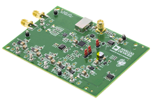
ADA4861-3YR-EBZ
Analog Devices Inc.The ADA4861-3 is a low cost, high speed, current feedback, triple op amp that provides excellent overall performance. The 730 MHz, -3 dB bandwidth, and 625 V/?s slew rate make this amplifier well suited for many high speed applications. With its combination of low price, excellent differential gain (0.01%), differential phase (0.02?), and 0.1 dB flatness out to 100 MHz, this amplifier is ideal for both consumer and professional video applications.The ADA4861-3 is designed to operate on supply voltages as low as +5 V and up to ?5 V using only 6 mA/amplifier of supply current. To further reduce power consumption, each amplifier is equipped with a power-down feature that lowers the supply current to 0.3 mA/amp when not being used.The ADA4861-3 is available in a 14-lead SOIC package and is designed to work over the extended temperature range of -40?C to +105?C.
ADA4950-1YCP-EBZ
Analog Devices Inc.The ADA4950-1/ADA4950-2 are gain-selectable versions of the ADA4932-1/ADA4932-2 with on-chip feedback and gain resistors with on-chip feedback and gain resistors. It is an ideal choice for driving high performance ADCs as a single-ended-to-differential or differential-to-differential amplifier. The output common-mode voltage is user adjustable by means of an internal common-mode feedback loop, allowing the ADA4950-x output to match the input of the ADC. The internal feedback loop also provides exceptional output balance as well as suppression of even-order harmonic distortion products.Differential gain configurations of 1, 2, and 3 are easily realized with internal feedback networks that are connected externally to set the closed-loop gain of the amplifier.The ADA4950-1/ADA4950-2 are fabricated using the Analog Devices, Inc., proprietary silicon-germanium (SiGe) complementary bipolar process, enabling them to achieve low levels of distortion and noise at low power consumption. The low offset and excellent dynamic performance of the ADA4950-x make it well suited for a wide variety of data acquisition and signal processing applications.The ADA4950-x is available in a Pb-free, 3 mm ? 3 mm, 16-lead LFCSP (ADA4950-1, single) or a Pb-free 4 mm ? 4 mm, 24-lead LFCSP (ADA4950-2, dual). The pinout has been optimized to facilitate PCB layout and minimize distortion. The ADA4950-1/ADA4950-2 are specified to operate over the -40?C to +105?C temperature range; both operate on supplies from +3 V to ?5 V.ApplicationsADC driversSingle-ended-to-differential convertersIF and baseband gain blocksDifferential buffersLine drivers
ADAR1000-EVALZ
Analog Devices Inc.The ADAR1000 is a 4-channel, X and Ku frequency band, beamforming core chip for phased arrays. This device operates in half-duplex between receive and transmit modes. In receive mode, input signals pass through four receive channels and are combined and output at the common RF_IO pin. In transmit mode, the RF_IO input signal is split and passes through the four transmit channels. In both modes, the ADAR1000 provides a ?31 dB gain adjustment range and a full 360? phase adjustment range in each radio frequency (RF) channel, with 6-bit resolution (less than ?0.5 dB and 2.8?, respectively).A simple 4-wire serial port interface (SPI) controls all of the on-chip registers. In addition, two address pins allow SPI control of up to four devices on the same serial lines. Dedicated transmit and receive load pins also provide synchronization of all ADAR1000 chips in the same array, and a single pin controls fast switching between the transmit and receive modes. The ADAR1000 is fabricated in a silicon-germanium, bipolar CMOS (BiCMOS) process. The device is available in a compact, 88-terminal, 7 mm ? 7 mm, LGA package and is specified from ?40?C to +85?C.APPLICATIONS Phased array radar Satellite communications systems
ADCA3270-EVALZ
Analog Devices Inc.The Analog Devices, Inc., ADCA3270 is a 24 V power doubler, monolithic microwave IC (MMIC) with 25 dB of power gain. The device achieves high RF output up to 73 dBmV composite power under 18 dB tilt conditions by using advanced circuit design techniques with gallium arsenide (GaAs), pseudomorphic high electron transistor (pHEMT), and gallium nitride (GaN) HEMT technologies. The dc current and supply voltage can be adjusted externally for optimum distortion performance vs. power consumption over a range of output levels. The ADCA3270 provides high gain, simplifying the design and manufacturing of DOCSIS 3.1 infrastructure equipment.The ADCA3270 is packaged in a 9-terminal thermally enhanced chip array small outline no lead cavity [LGA_CAV] with an industry-standard footprint.APPLICATIONS45 MHz to 1218 MHz community access television (CATV) infrastructure amplifier systemsRemote physical layer (PHY)DOCSIS 3.1 compliant
ADCLK948/PCBZ
Analog Devices Inc.The ADCLK948 is an ultrafast clock fanout buffer fabricated on the Analog Devices, Inc., proprietary XFCB3 silicon germanium (SiGe) bipolar process. This device is designed for high speed applications requiring low jitter.The device has two selectable differential inputs via the IN_SEL control pin. Both inputs are equipped with center tapped, differential, 100 ? on-chip termination resistors. The inputs accept dc-coupled LVPECL, CML, 3.3 V CMOS (single-ended), and ac-coupled 1.8 V CMOS, LVDS, and LVPECL inputs. A VREFx pin is available for biasing ac-coupled inputs. The ADCLK948 features eight full-swing emitter coupled logic(ECL) output drivers. For LVPECL (positive ECL) operation, bias VCC to the positive supply and VEE to ground. For ECL operation, bias VCC to ground and VEE to the negative supply.The output stages are designed to directly drive 800 mV eachside into 50 ? terminated to VCC -2V for a total differential output swing of 1.6V. The ADCLK948 is available in a 32-lead LFCSP and specified for operation over the standard industrial temperature range of ?40?C to +85?C.APPLICATIONS Low jitter clock distribution Clock and data signal restoration Level translation Wireless communications Wired communications Medical and industrial imaging ATE and high performance instrumentation
ADF70301-915EZKIT
Analog Devices Inc.The ADF7030-1 is a fully integrated, radio transceiver achieving high performance at very low power. The ADF7030-1 is ideally suited for applications that require long range, network robustness, and long battery life. It is suitable for applications that operate in the ISM, SRD, and licensed frequency bands at 169.4 MHz to 169.6 MHz, 426 MHz to 470 MHz, and 863 MHz to 960 MHz. It provides extensive support for standards-based protocols like IEEE802.15.4g while also providing flexibility to support a wide range of proprietary protocols.The highly configurable low intermediate frequency (IF) receiver supports a large range of receiver channel bandwidths from 2.6 kHz to 406 kHz. This range of receiver channel bandwidths allows the ADF7030-1 to support ultranarrow-band, narrow-band, and wideband channel spacing.The ADF7030-1 features two independent PAs supporting output power ranges of ?20 dBm to +13 dBm and ?20 dBm to +17 dBm. The PAs support ultrafine adjustment of the power with a step resolution of 0.1 dB. The PA output power is exceptionally robust over temperature and voltage. The PAs have an automatic power ramp control to limit spectral splatter to meet regulatory standards.The ADF7030-1 features an on-chip ARM??Cortex?-M0 processor that performs radio control, radio calibration, and packet management. Cortex-M0 eases the processing burden of the host processor because the ADF7030-1 integrates the lower layers of a typical communication protocol stack. This internal processor also permits the download and execution of Analog Devices, Inc., provided firmware modules that can extend the functionality of the ADF7030-1.The ADF7030-1 has two packet modes: generic packet mode and IEEE802.15.4g mode. In generic packet mode, the packet format is highly flexible and fully programmable, thereby ensuring its compatibility with proprietary packet formats. In IEEE802.15.4g packet mode, the packet format conforms to the?IEEE802.15.4g standard. FEC, as per the IEEE802.15.4g standard, is also supported.The ADF7030-1 operates with a power supply range of 2.2 V to 3.6 V and has very low power consumption in both Tx and Rx modes, enabling long lifetimes in battery-operated systems. An ultralow power deep sleep mode achieves a typical current of 10 nA with the configuration memory retained.A complete wireless solution can be built using a small number of external discrete components and a host processor (typically a microcontroller). The host processor can configure the ADF7030-1 using a simple command-based protocol over a standard 4-wire SPI interface. A single-byte command transitions the radio between states or performs a radio function.The ADF7030-1 is available in two package types: a 6 mm ? 6 mm, 40-lead LFCSP and a 7 mm ? 7 mm, 48-lead LQFP. Both package types use NiPdAu plating to mitigate against silver migration in high humidity applications. The ADF7030-1 operating temperature range is ?40?C to +85?C.For Figure 13 to Figure 19, Figure 30, Figure 42, Figure 60, Figure 61, and Figure 75 in the Typical Performance Characteristics section, PA_COARSE is a programmable value that provides a coarse adjustment of the PA output power. This value can be programmed in the range of 1 to 6 for PA1, and from 1 to 10 for PA2. PA_FINE is a programmable value that provides a fine adjustment of the PA output power. This value can be programmed in the range of 3 to 127 for both PA1 and PA2. PA_MICRO is a programmable value that provides a microadjustment (typically
AD-FMCADC20-DC-EBZ
Analog Devices Inc.The ADL5580 is a high performance, single-ended or differential amplifier with 10 dB of voltage gain, optimized for applications spanning from dc to 10.0 GHz. The amplifier offers a low referred to input (RTI) noise spectral density (NSD) of 2.24 nV/?Hz (at 1000 MHz) and is optimized for distortion performance over a wide frequency range, making the device an ideal driver for high speed 12-bit to 16-bit analog-to-digital converters (ADCs). The ADL5580 is suited for use in high performance, zero intermediate frequency (IF), and complex IF receiver designs. In addition, this device has low distortion for single-ended input driver applications.By using two external series resistors, the gain selection from 10 dB for a differential input can be modified to a lower gain. The device maintains low distortion through its output common-mode voltage (VCM) of 0.5 V, providing a flexible capability for driving ADCs with full-scale levels up to 1.4 V p-p.Operating from a +5 V and ?1.8 V supply, the positive and negative supply current of the ADL5580 is typically +276 mA and ?224 mA, respectively. The device has a power disable feature, and when disabled, the amplifier consumes 2 mA.The ADL5580 is optimized for wideband, low distortion, and low noise operation at the dc to 10.0 GHz frequency range. These attributes, together with its adjustable gain capability, make this device an optimal choice for driving a wide variety of ADCs, mixers, pin diode attenuators, surface acoustic wave (SAW) filters, and a multiplicity of discrete RF devices.Fabricated on an Analog Devices, Inc., high speed silicon germanium (SiGe) process, the ADL5580 is supplied in a compact 4 mm ? 4 mm, 20-terminal land grid array (LGA)package and operates over the ?40?C to +85?C temperature range.APPLICATIONSInstrumentation and defense applications
ADIS16201/PCBZ
Analog Devices Inc.The ADIS16201 is a complete, dual-axis acceleration and inclination angle measurement system available in a single compact package enabled by the Analog Devices iSensor? integration. By enhancing the Analog Devices iMEMS? sensor technology with an embedded signal processing solution, the ADIS16201 provides factory calibrated and tunable digital sensor data in a convenient format that can be accessed using a serial peripheral interface (SPI). The SPI interface provides access to measurements for dual-axis linear acceleration, dual-axis linear inclination angle, temperature, power supply, and one auxiliary analog input. Easy access to calibrated digital sensor data provides developers with a system-ready device, reducing development time, cost, and program risk.Unique characteristics of the end system are accommodated easily through several built-in features, such as a single command in-system offset calibration, along with convenient sample rate and bandwidth control.The ADIS16201 offers the following embedded features, which eliminate the need for external circuitry and provide a simplified system interface: Configurable alarm function Auxiliary 12-bit ADC Auxiliary 12-bit DAC Configurable digital I/O port Digital self-test functionThe ADIS16201 offers two power management features for managing system-level power dissipation: low power mode and a configurable shutdown feature.The ADIS16201 is available in a 9.2 mm ? 9.2 mm ? 3.9 mm laminate-based land grid array (LGA) package with a temperature range of ?40?C to +125?C.APPLICATIONS Platform control, stabilization, and leveling Tilt sensing, inclinometers Motion/position measurement Monitor/alarm devices (security, medical, safety)
ADIS16475-3/PCBZ
Analog Devices Inc.The ADIS16475 is a precision, miniature MEMS inertial measurement unit (IMU) that includes a triaxial gyroscope and a triaxial accelerometer. Each inertial sensor in the ADIS16475 combines with signal conditioning that optimizes dynamic performance. The factory calibration characterizes each sensor for sensitivity, bias, alignment, linear acceleration (gyroscope bias), and point of percussion (accelerometer location). As a result, each sensor has dynamic compensation formulas that provide accurate sensor measurements over a broad set of conditions.The ADIS16475 provides a simple, cost effective method for integrating accurate, multiaxis inertial sensing into industrial systems, especially when compared with the complexity and investment associated with discrete designs. All necessary motion testing and calibration are part of the production process at the factory, greatly reducing system integration time. Tight orthogonal alignment simplifies inertial frame alignment in navigation systems. The serial peripheral interface (SPI) and register structure provide a simple interface for data collection andconfiguration control.The ADIS16475 is available in a 44-ball, ball grid array (BGA) package that is approximately 11 mm ? 15 mm ? 11 mm.Applications Navigation, stabilization, and instrumentation Unmanned and autonomous vehicles Smart agriculture and construction machinery Factory/industrial automation, robotics Virtual/augmented reality Internet of Moving Things
ADIS16477-2/PCBZ
Analog Devices Inc.The ADIS16477 is a precision, miniature MEMS inertial measurement unit (IMU) that includes a triaxial gyroscope and a triaxial accelerometer. Each inertial sensor in the ADIS16477 combines with signal conditioning that optimizes dynamic performance. The factory calibration characterizes each sensor for sensitivity, bias, alignment, linear acceleration (gyroscope bias), and point of percussion (accelerometer location). As a result, each sensor has dynamic compensation formulas that provide accurate sensor measurements over a broad set of conditions.The ADIS16477 provides a simple, cost effective method for integrating accurate, multiaxis inertial sensing into industrial systems, especially when compared with the complexity and investment associated with discrete designs. All necessary motion testing and calibration are part of the production process at the factory, greatly reducing system integration time. Tight orthogonal alignment simplifies inertial frame alignment in navigation systems. The serial peripheral interface (SPI) and register structure provide a simple interface for data collection and configuration control.The ADIS16477 is available in a 44-ball, ball grid array (BGA) package that is approximately 11 mm ? 15 mm ? 11 mm.Applications Navigation, stabilization, and instrumentation Unmanned and autonomous vehicles Smart agriculture/construction machinery Factory/industrial automation, robotics Virtual/augmented reality Internet of Moving Things
ADIS16505-1/PCBZ
Analog Devices Inc.The ADIS16505 is a precision, miniature microelectromechanical system (MEMS) inertial measurement unit (IMU) that includes a triaxial gyroscope and a triaxial accelerometer. Each inertial sensor in the ADIS16505 combines with signal conditioning that optimizes dynamic performance. The factory calibration characterizes each sensor for sensitivity, bias, alignment, linear acceleration (gyroscope bias), and point of percussion (accelerometer location). As a result, each sensor has dynamic compensation formulas that provide accurate sensor measurements over a broad set of conditions.The ADIS16505 provides a simplified, cost effective method for integrating accurate, multi-axis inertial sensing into industrial systems, especially when compared with the complexity and investment associated with discrete designs. All necessary motion testing and calibration are part of the production process at the factory, greatly reducing system integration time. Tight orthogonal alignment simplifies inertial frame alignment in navigation systems. The serial peripheral interface (SPI) and register structure provide a simple interface for data collection and configuration control.The ADIS16505 is available in a 100-ball, ball grid array (BGA) package that is approximately 15 mm ? 15 mm ? 5 mm.Applications Navigation, stabilization, and instrumentation Unmanned and autonomous vehicles Smart agriculture and construction machinery Factory/industrial automation, robotics Virtual/augmented reality Internet of Moving Things
ADIS16507-2/PCBZ
Analog Devices Inc.The ADIS16507 is a precision, miniature microelectromechanical?system (MEMS) inertial measurement unit (IMU) that includes?a triaxial gyroscope and a triaxial accelerometer. Each inertial?sensor in the ADIS16507 combines with signal conditioning?that optimizes dynamic performance. The factory calibration?characterizes each sensor for sensitivity, bias, alignment,?linear acceleration (gyroscope bias), and point of percussion?(accelerometer location). As a result, each sensor has dynamic?compensation formulas that provide accurate sensor?measurements over a broad set of conditions.The ADIS16507 provides a simplified, cost effective method for?integrating accurate, multiaxis inertial sensing into industrial?systems, especially when compared with the complexity and?investment associated with discrete designs. All necessary motion?testing and calibration are part of the production process at the?factory, greatly reducing system integration time. Tight orthogonal?alignment simplifies inertial frame alignment in navigation?systems. The serial peripheral interface (SPI) and register?structure provide a simple interface for data collection and?configuration control.The ADIS16507 is available in a 100-ball, ball grid array (BGA)?package that is approximately 15 mm ? 15 mm ? 5 mm.Applications Navigation, stabilization, and instrumentation Unmanned and autonomous vehicles Smart agriculture and construction machinery Factory/industrial automation, robotics Virtual/augmented reality Internet of Moving Things
ADL5240-EVALZ
Analog Devices Inc.The ADL5240 is a high performance, digitally controlled variable gain amplifier (VGA) operating from 100 MHz to 4000 MHz. The VGA integrates a high performance, 20 dB gain, internally matched amplifier (AMP) with a 6-bit digital step attenuator (DSA) that has a gain control range of 31.5 dB in 0.5 dB steps with ?0.25 dB step accuracy. The attenuation of the DSA can be controlled using a serial or parallel interface.Both the gain block and DSA are internally matched to 50 ? at their inputs and outputs and are separately biased. The separate bias allows all or part of the ADL5240 to be used, which facilitates easy reuse throughout a design. The pinout of the ADL5240 also enables either the gain block or DSA to be first, giving the VGA maximum flexibility in a signal chain.The ADL5240 consumes just 93 mA and operates from a single supply ranging from 4.75 V to 5.25 V. The VGA is packaged in a thermally efficient, 5 mm ? 5 mm, 32-lead LFCSP and is fully specified for operation from ?40?C to +85?C. A fully populated evaluation board is available.ApplicationsWireless infrastructureAutomated test equipmentRF/IF gain control
ADL5246-EVALZ
Analog Devices Inc.The ADL5246 is a high performance, low noise variable gain amplifier (VGA) optimized for multistandard base station receivers and point to point receive (Rx) and transmit (Tx) applications. The low noise figure and excellent linearity performance allow the device to be used in a variety of applications.The device consists of a low noise amplifier, a high linearity VGA, and a ? W output driver stage. The variable attenuator networks are optimized to provide high linearity performance over the 45 dB gain control range. Gain is set using a unipolar control voltage from 0 V to 3.3 V. The output stage of the ADL5246 is an externally tuned ? W driver amplifier, which allows the device to be optimized anywhere between the 0.6 GHzto 3 GHz range, with an average tuning bandwidth of 200 MHz wide. An external filter can be used between the VGA and the final driver amplifier. The ADL5246 can be biased between 3.3 V and 5 V to tradeoff between performance and power consumption.The ADL5246 is fabricated on an advanced GaAs process. The device is available in a 32-lead, RoHS-compliant, 5 mm ? 5 mm LFCSP and thermally rated to operate over the ?40?C to +105?C temperature range.APPLICATIONS Multistandard radio receivers Point to point Rx and Tx Instrumentation Military and aerospace
ADL5310-EVALZ
Analog Devices Inc.The ADL5310 is a low-cost dual logarithmic amplifier that converts input current over a wide dynamic range to a linear-in-dB output voltage. It is optimized for the determination of optical power in wide-ranging optical communication system applications including control circuitry for lasers, optical switches, attenuators, and amplifiers, as well as general system monitoring. The device is equivalent to a dual AD8305 with enhanced dynamic range (120 dB). While the ADL5310 contains two independent signal channels with individually-configurable transfer function constants (slope and intercept), internal bias circuitry is shared between channels for improved power consumption and channel matching. Dual converters in a single compact LFCSP package yield space-efficient solutions for measuring gain or attenuation across optical elements. Only a single supply is required, while optional dual supply operation offers added flexibility.The ADL5310 employs an optimized translinear structure, which utilizes the accurate logarithmic relationship between a bipolar transistor's base-emitter voltage and collector current, with appropriate scaling by precision currents to compensate the inherent temperature dependence. Input and reference current pins sink current ranging from 3 nA to 3 mA (limited to ?60 dB between input and reference) into a fixed voltage defined by the VSUM potential, which is internally set to 500 mV but may be externally-grounded for dual-supply operation and additional applications requiring voltage inputs.
ADL5324-EVALZ
Analog Devices Inc.The ADL5324 incorporates a dynamically adjustable biasing circuit that allows for the customization of OIP3 and P1dB performance from 3.3 V to 5 V, without the need for an external bias resistor. This feature gives the designer the ability to tailor driver amplifier performance to the specific needs of the design. This feature also creates the opportunity for dynamic biasing of the driver amplifier where a variable supply is used to allow for full 5 V biasing under large signal conditions, and then reduced supply voltage when signal levels are smaller and lower power consumption is desirable. This scalability reduces the need to evaluate and inventory multiple driver amplifiers for different output power requirements, from 25 dBm to 29 dBm output power levels.The ADL5324 is also rated to operate across the wide temperature range of ?40?C to +105?C for reliable performance in designs that experience higher temperatures, such as power amplifiers. The ? W driver amplifier also covers the wide frequency range of 400 MHz to 4000 MHz, and only requiresa few external components to be tuned to a specific band within that wide range. This high performance broadband RF driver amplifier is well suited for a variety of wired and wireless applications, including cellular infrastructure, ISM band power amplifiers, defense equipment, and instrumentation equipment. A fully populated evaluation board is available.The ADL5324 also delivers excellent ACPR vs. output power and bias voltage. The driver can deliver greater than 17 dBm of output power at 2140 MHz, while achieving an ACPR of ?55 dBc at 5 V. If the bias is reduced to 3.3 V, the ?55 dBc ACPR output power only minimally reduces to 15 dBm.Applications Wireless infrastructure Automated test equipment ISM/AMR applications
ADL5331-EVALZ
Analog Devices Inc.The ADL5331 is a high performance, voltage-controlledvariable gain amplifier/attenuator for use in applications with frequencies up to 1.2 GHz. The balanced structure of the signal path maximizes signal swing, eliminates common-mode noiseand minimizes distortion while it also reduces the risk of spurious feed-forward at low gains and high frequencies caused by parasitic coupling. The 50 ? differential input system converts the applieddifferential voltage at INHI and INLO to a pair of differentialcurrents with high linearity and good common-mode rejection. The signal currents are then applied to a proprietary voltage-controlled attenuator providing precise definition of the overall gain under the control of the linear-in-dB interface. The GAIN pin accepts a voltage from 0 V at a minimum gain to 1.4 V at afull gain with a 40 mV/dB scaling factor over most of the range.The output of the high accuracy wideband attenuator is appliedto a differential transimpedance output stage. The output stageprovides a differential output at OPHI and OPLO, which must be pulled up to the supply with RF chokes or a center-tapped balun.The ADL5331 consumes 240 mA of current including the output pins and operates off a single supply ranging from 4.75 V to 5.25 V. A power-down function is provided by applying alogic low input on the ENBL pin. The current consumption inpower-down mode is 250 ?A.The ADL5331 is fabricated on an Analog Devices, Inc., proprietary high performance, complementary bipolar IC process.The ADL5331 is available in a 24-lead (4 mm ? 4 mm), Pb-freeLFCSP package and is specified for operation from ambient temperatures of ?40?C to +85?C. An evaluation board is also available.Applications Transmit and receive power control at RF and IF CATV distribution
ADL5375-05EP-EVALZ
Analog Devices Inc.The ADL5375 is a broadband quadrature modulator designed for operation from 400 MHz to 6 GHz. Its excellent phase accuracy and amplitude balance enable high performance intermediate frequency or direct radio frequency modulation for communication systems.The ADL5375 features a broad baseband bandwidth, along with an output gain flatness that varies no more than 1 dB from 450 MHz to 3.8 GHz. These features, coupled with a broadband output return loss of
ADL5382-EVALZ
Analog Devices Inc.The ADL5382 is a broadband quadrature I-Q demodulator that covers an RF input frequency range from 700 MHz to 2.7 GHz. With a NF = 14 dB, IP1dB = 14.7 dBm, and IIP3 = 33.5 dBm at 900 MHz, the ADL5382demodulator offers outstanding dynamic range suitable for the demanding infrastructure direct-conversion requirements. The differential RF inputs provide a well-behaved broadband input impedance of 50 ? and are best driven from a 1:1 balun for optimum performance.Excellent demodulation accuracy is achieved with amplitude and phase balances ~0.05 dB and ~0.2?, respectively. The demodulated in-phase (I) and quadrature (Q) differential outputs are fully buffered and provide a voltage conversion gain of ~4 dB. The buffered baseband outputs are capable of driving a 2 Vp-p differential signal into 200 ?.The fully balanced design minimizes effects from second-order distortion. The leakage from the LO port to the RF port is 60 dBm.The ADL5382 operates off a single 4.75 V to 5.25 V supply. The supply current is adjustable with an external resistor from the BIAS pin to ground.The ADL5382 is fabricated using the Analog Devices, Inc., advanced Silicon-Germanium bipolar process and is available in a 24-lead exposed paddle LFCSP. Performance is specified over a -40?C to +85?C temperature range.APPLICATIONS QAM/QPSK demodulator W-CDMA/CDMA/CDMA2000/GSM Point-to-(Multi)Point Radio WiMax
ADL5390-EVALZ
Analog Devices Inc.The ADL5390 vector multiplier consists of a matched pair of broadband variable gain amplifiers whose outputs are summed. The separate gain controls for each amplifier are linear-in-magnitude. If the two input RF signals are in quadrature, the vector multiplier can be configured as a vector modulator or as a variable attenuator/phase shifter by using the gain control pins as Cartesian variables. In this case, the output amplitude can be controlled from a maximum of +5 dB to less than -30 dB, and the phase can be shifted continuously over the entire 360? range. Since the signal paths are linear, the original modulation on the inputs is preserved. If the two signals are independent, then the vector multiplier can function as a 2:1 multiplexer or can provide fading from one channel to another.The ADL5390 operates over a wide frequency range of 20 MHz to 2400 MHz. For a maximum gain setting on one channel at 380 MHz, the ADL5390 delivers an OP1dB of 11 dBm, an OIP3 of 24 dBm, and an output noise floor of -148 dBm/Hz. The gain and phase matching between the two VGAs is better than 0.5 dB and 1?, respectively, over most of the operating range.The ADL5390 is fabricated on Analog Devices' proprietary, high performance 25 GHz SOI complementary bipolar IC process. It is available in a 24-lead, Pb-free CSP package and operates over a -40?C to +85?C temperature range. Evaluation boards are available.APPLICATIONS PA linearization and predistortion Amplitude and phase modulation Variable matched attenuator and/or phase shifter Cellular base stations Radio links Fixed wireless access Broadband/CATV RF/IF analog multiplexerAVAILABILITYSamples, part number ADL5390ACPZ, and an evaluation board, part number ADL5390-EVAL, are available.COMPANION PRODUCTSAD8302 - LF to 2.7GHz RF/IF Gain Phase DetectorAD8340 - RF Vector Modulator 700MHz to 1000MHzAD8341 - RF Vector Modulator 1.5GHz to 2.4GHz


