Top Manufacturers
Stock

Displaying 3381 - 3400 of 5453

Evaluation Kits from Analog Devices Inc.

EVAL-ADUC7061MKZ

Analog Devices Inc.
The ADuC7060/ADuC7061 are fully integrated, 8 kSPS, 24-bit data acquisition systems incorporating high performance multi-channel sigma-delta (?-?) analog-to-digital converters (ADCs), 16-bit/ 32-bit ARM7TDMI? MCU, and Flash/EE memory on a single chip.The ADCs consists of a 5-channel primary ADC and up to an 8-channel auxiliary ADC. The ADCs operate in single-ended or differential input modes. A single channel buffered voltage output DAC is available on-chip. The DAC output range is programmable to one of two voltage ranges.The devices operate from an on-chip oscillator and a PLL gene-rating an internal high frequency clock up to 10.24 MHz. The microcontroller core is an ARM7TDMI, 16-bit/32-bit RISC machine offering up to 10 MIPS peak performance. 4 kB of SRAM and 32 kB of nonvolatile Flash/EE memory are provided on-chip. The ARM7TDMI core views all memory and registers as a single linear array.The ADuC7060/ADuC7061 contain four timers. Timer 1 is wake-up timer with the ability to bring the part out of power saving mode. Timer 2 may be configured as a watchdog timer. A 16-bit PWM with six output channels is also provided.The ADuC7060/ADuC7061 contain an advanced interrupt controller. The vectored interrupt controller (VIC) allows every interrupt to be assigned a priority level. It also supports nested interrupts to a maximum level of eight per IRQ and FIQ. When IRQ and FIQ interrupt sources are combined, a total of 16 nested interrupt levels are supported. On-chip factory firmware supports in-circuit serial download via the UART serial interface ports and nonintrusive emulation via the JTAG interface.The parts operate from 2.375 V to 2.625 V over an industrial temperature range of ?40?C to +125?C.Applications Industrial automation and process control Intelligent, precision sensing systems, 4 mA to 20 mA loop-based smart sensors

EVAL-ADUC841QSPZ

Analog Devices Inc.
The ADuC841/ADuC842/ADuC843 are complete smart transducer front ends, that integrates a high performance self-calibrating multichannel ADC, a dual DAC, and an optimized single-cycle 20 MHz 8-bit MCU (8051 instruction set compatible)on a single chip.The ADuC841 and ADuC842 are identical with the exception of the clock oscillator circuit; the ADuC841 is clocked directly from an external crystal up to 20 MHz whereas the ADuC842 uses a 32 kHz crystal with an on-chip PLL generating a programmable core clock up to 16.78 MHz.The ADuC843 is identical to the ADuC842 except that the ADuC843 has no analog DAC outputs.The microcontroller is an optimized 8052 core offering up to 20 MIPS peak performance. Three different memory options are available offering up to 62 kBytes of nonvolatile Flash/EE program memory. Four kBytes of nonvolatile Flash/EE data memory, 256 bytes RAM, and 2 kBytes of extended RAM are also integrated on-chip. The parts also incorporate additional analog functionality with two 12-bit DACs, power supply monitor, and a band gap reference. On-chip digital peripherals include two 16-bit ?-?. DACs, a dual output 16-bit PWM, a watchdog timer, a time interval counter, three timers/counters, and three serial I/O ports (SPI, I2C, and UART).On the ADuC812 and the ADuC832, the I2C and SPI interfaces share some of the same pins. For backwards compatibility, this is also the case for the ADuC841/ADuC842/ADuC843.However, there is also the option to allow SPI operate separately on P3.3, P3.4, and P3.5, while I2C uses the standard pins. The I2C interface has also been enhanced to offer repeated start, general call, and quad addressing.On-chip factory firmware supports in-circuit serial download and debug modes (via UART) as well as single-pin emulation mode via the EA pin..Applications Optical networking?laser power control Base station systems Precision instrumentation, smart sensors Transient capture systems DAS and communications systems

EVAL-ADUC842QSPZ

Analog Devices Inc.
The ADuC841/ADuC842/ADuC843are complete smart transducer front ends, that integrates a high performance self-calibrating multichannel ADC, a dual DAC, and an optimized single-cycle 20 MHz 8-bit MCU (8051 instruction set compatible)on a single chip.The ADuC841 and ADuC842 are identical with the exception of the clock oscillator circuit; the ADuC841 is clocked directly from an external crystal up to 20 MHz whereas the ADuC842 uses a 32 kHz crystal with an on-chip PLL generating aprogrammable core clock up to 16.78 MHz.The ADuC843 is identical to the ADuC842 except that the ADuC843 has no analog DAC outputs.The microcontroller is an optimized 8052 core offering up to 20 MIPS peak performance. Three different memory options are available offering up to 62 kBytes of nonvolatile Flash/EE program memory. Four kBytes of nonvolatile Flash/EE data memory, 256 bytes RAM, and 2 kBytes of extended RAM arealso integrated on-chip. The parts also incorporate additional analog functionality with two 12-bit DACs, power supply monitor, and a band gap reference. On-chip digital peripherals include two 16-bit ?-?. DACs, a dual output 16-bit PWM, a watchdog timer, a time interval counter, three timers/counters, and three serial I/O ports (SPI, I2C, and UART).On the ADuC812 and the ADuC832, the I2C and SPI interfaces share some of the same pins. For backwards compatibility, this is also the case for the ADuC841/ADuC842/ADuC843.However, there is also the option to allow SPI operate separately on P3.3, P3.4, and P3.5, while I2C uses the standard pins. The I2C interface has also been enhanced to offer repeated start, general call, and quad addressing.On-chip factory firmware supports in-circuit serial download and debug modes (via UART) as well as single-pin emulation mode via the EA pin.Applications Optical networking?laser power control Base station systems Precision instrumentation, smart sensors Transient capture systems DAS and communications systems

EVAL-ADUC845QSPZ

Analog Devices Inc.
The ADuC845, ADuC847, and ADuC848 are single-cycle,12.58 MIPs, 8052 core upgrades to the ADuC834 andADuC836. They include additional analog inputs forapplications requiring more ADC channels.The ADuC845, ADuC847, and ADuC848 are complete smarttransducer front ends. The family integrates high resolution?-? ADCs with flexible, up to 10-channel, input multiplexing, afast 8-bit MCU, and program and data Flash/EE memory on asingle chip.The ADuC845 includes two (primary and auxiliary) 24-bit ?-?ADCs with internal buffering and PGA on the primary ADC.The ADuC847 includes the same primary ADC as the ADuC845(auxiliary ADC removed). The ADuC848 is a 16-bit ADCversion of the ADuC847.The ADCs incorporate flexible input multiplexing, a temperaturesensor (ADuC845 only), and a PGA (primary ADC only)allowing direct measurement of low-level signals. The ADCsinclude on-chip digital filtering and programmable output datarates that are intended for measuring wide dynamic range andlow frequency signals, such as those in weigh scale, strain gage,pressure transducer, or temperature measurement applications.The devices operate from a 32 kHz crystal with an on-chip PLLgenerating a high frequency clock of 12.58 MHz. This clock isrouted through a programmable clock divider from which theMCU core clock operating frequency is generated. The microcontrollercore is an optimized single-cycle 8052 offering up to12.58 MIPs performance while maintaining 8051 instruction setcompatibility.The available nonvolatile Flash/EE program memory optionsare 62 kbytes, 32 kbytes, and 8 kbytes. 4 kbytes of nonvolatileFlash/EE data memory and 2304 bytes of data RAM are alsoprovided on-chip. The program memory can be configured asdata memory to give up to 60 kbytes of NV data memory indata logging applications.On-chip factory firmware supports in-circuit serial downloadand debug modes (via UART), as well as single-pin emulationmode via the EA pin. The ADuC845, ADuC847, and ADuC848are supported by the QuickStart? development system featuringlow cost software and hardware development tools.Applications Multichannel sensor monitoring Industrial/environmental instrumentation Weigh scales, pressure sensors, temperature monitoring Portable instrumentation, battery-powered systems Data logging, precision system monitoring

EVAL-ADUC845QSZ

Analog Devices Inc.
The ADuC845, ADuC847, and ADuC848 are single-cycle,12.58 MIPs, 8052 core upgrades to the ADuC834 andADuC836. They include additional analog inputs forapplications requiring more ADC channels.The ADuC845, ADuC847, and ADuC848 are complete smarttransducer front ends. The family integrates high resolution?-? ADCs with flexible, up to 10-channel, input multiplexing, afast 8-bit MCU, and program and data Flash/EE memory on asingle chip.The ADuC845 includes two (primary and auxiliary) 24-bit ?-?ADCs with internal buffering and PGA on the primary ADC.The ADuC847 includes the same primary ADC as the ADuC845(auxiliary ADC removed). The ADuC848 is a 16-bit ADCversion of the ADuC847.The ADCs incorporate flexible input multiplexing, a temperaturesensor (ADuC845 only), and a PGA (primary ADC only)allowing direct measurement of low-level signals. The ADCsinclude on-chip digital filtering and programmable output datarates that are intended for measuring wide dynamic range andlow frequency signals, such as those in weigh scale, strain gage,pressure transducer, or temperature measurement applications.The devices operate from a 32 kHz crystal with an on-chip PLLgenerating a high frequency clock of 12.58 MHz. This clock isrouted through a programmable clock divider from which theMCU core clock operating frequency is generated. The microcontrollercore is an optimized single-cycle 8052 offering up to12.58 MIPs performance while maintaining 8051 instruction setcompatibility.The available nonvolatile Flash/EE program memory optionsare 62 kbytes, 32 kbytes, and 8 kbytes. 4 kbytes of nonvolatileFlash/EE data memory and 2304 bytes of data RAM are alsoprovided on-chip. The program memory can be configured asdata memory to give up to 60 kbytes of NV data memory indata logging applications.On-chip factory firmware supports in-circuit serial downloadand debug modes (via UART), as well as single-pin emulationmode via the EA pin. The ADuC845, ADuC847, and ADuC848are supported by the QuickStart? development system featuringlow cost software and hardware development tools.Applications Multichannel sensor monitoring Industrial/environmental instrumentation Weigh scales, pressure sensors, temperature monitoring Portable instrumentation, battery-powered systems Data logging, precision system monitoring

EVAL-ADUCM310QSPZ

Analog Devices Inc.
The ADuCM310 is a multidie stack, on-chip system designed for diagnostic control of tunable laser optical module applications. The ADuCM310 features a 16-bit (14-bit accurate) multichannel successive approximation register (SAR) ADC, an ARM Cortex?-M3 processor, eight voltage DACs (VDACs), six current output DACs, and Flash/EE memory packaged in a 6 mm ? 6 mm, 112-ball CSP_BGA package.The bottom die in the stack supports the bulk of the low voltage analog circuitry and is the largest of the three die. It contains the ADC, VDACs, main IDAC circuits, as well as other analog support circuits, such as the low drift precision 2.5 V voltage reference source.The middle die in the stack supports the bulk of the digital circuitry, including the ARM Cortex-M3 processor, the flash and SRAM blocks, and all of the digital communication peripherals. In addition, this die provides the clock sources for the whole chip. A 16 MHz internal oscillator is the source of the internal PLL that outputs an 80 MHz system clock.The top die, which is the smallest die, was developed on a high voltage process, and this die supports the ?5 V and +5 V VDAC outputs. It also implements the SOA IDAC current sink circuit that allows the external SOA diode to pull to a ?3.0 V level to implement the fast shutdown of the laser output.Regarding the individual blocks, the ADC is capable of operating at conversion rates up to 800 kSPS. There are 10 external inputs to the ADC, which can be single ended or differential. Several internal channels are included, such as the supply monitor channels, an on-chip temperature sensor, and internal voltage reference monitors.The VDACs are 12-bit string DACs with output buffers capable of sourcing between 10 mA and 50 mA, and these DACs are all capable of driving 10 nF capacitive loads.The low drift current DACs have 14-bit resolution and varied full-scale output ranges from 0 mA to 20 mA to 0 mA to 250 mA on the SOA IDAC (IDAC3). The SOA IDAC also comes with a 0 mA to ?80 mA current sink capability.A precision 2.5 V on-chip reference source is available. The internal ADC, IDACs, and VDAC circuits use this on-chip reference source to ensure low drift performance for all of these peripherals.The ADuCM310 also provides 2? buffered reference outputs capable of sourcing up to 1.2 mA. These outputs can be used externally to the chip.The ADuCM310 integrates an 80 MHz ARM Cortex-M3 processor. It is a 32-bit reduced instruction set computer (RISC) machine, offering up to 100 DMIPS peak performance. The ARM Cortex-M3 processor also has a flexible 14-channel direct memory access (DMA) controller supporting serial peripheral interface (SPI), UART, and I2C communication peripherals. The ADuCM310 has 256 kB of nonvolatile Flash/EE memory and 32 kB of SRAM integrated on-chip.A 16 MHz on-chip oscillator generates the 80 MHz system clock. This clock internally divides to allow the processor to operate at lower frequency, thus saving power. A low power internal 32 kHz oscillator is available and can clock the timers. The ADuCM310 includes three general-purpose timers, a wake-up timer (which can be used as a general-purpose timer), and a system watchdog timer.A range of communication peripherals can be configured as required in a specific application. These peripherals include UART, 2 ? I2C, 2 ? SPI, GPIO ports, and pulse-width modulation (PWM).On-chip factory firmware supports in-circuit serial download via the UART, while nonintrusive emulation and program download are supported via the serial wire debug port (SW-DP) interface. These features are supported on the EVAL-ADuCM310QSPZ development system.The ADuCM310 operates from 2.9 V to 3.6 V and is specified over a temperature range of ?40?C to +85?C.Note that, throughout this data sheet, multifunction pins, such as P1.0/SIN/ECLKIN/PLAI[4], are referred to either by the entire pin name or by a single function of the pin, for example, P1.0, when only that function is relevant.For additional information on the ADuCM310, see the ADuCM310 reference manual, How to Set Up and Use the ADuCM310.APPLICATIONS Optical modules?tunable laser modules

EVAL-ADUCM350EBZ

Analog Devices Inc.
The ADuCM350 is a configurable Impedance Converter and Potentiostat with current and voltage measurement capability for both Electrochemical sensors and Biosensors. It is a complete, coin cell powered, high precision, MCU integrated solution for portable device applications such as point-of-care diagnostics and body-worn devices for monitoring vital signs.The ADuCM350 analog front end (AFE) features a 16-bit, precision, 160 kSPS analog-to-digital converter (ADC); 0.17% precision voltage reference; 12-bit, no missing codes digital-to-analog converter (DAC); and a reconfigurable ultralow leakage switch matrix. It has 4 voltage measurement channels, up to 8 current measurement channels and an impedance measurement DFT engine. The ADuCM350 also includes an ARM Cortex-M3-based processor, memory, and all I/O connectivity to support portable meters with display, USB communication, and active sensors. The ADuCM350 is available in a 120-lead, 8 mm ? 8 mm CSP_BGA and operates from ?40?C to +85?C. To support extremely low dynamic and hibernate power management, the ADuCM350 provides a collection of power modes and features, such as dynamic and software controlled clock gating and power gating.The AFE is connected to the ARM Cortex-M3 via an advanced high performance bus (AHPB) slave interface on the advanced microcontroller bus architecture (AMBA) matrix, as well as direct memory access (DMA) and interrupt connections.APPLICATIONS Point-of-care diagnostics Body-worn devices for monitoring vital signs Amperometric, voltametric, and impedometric measurements

EVAL-ADUCM355EMCZ

Analog Devices Inc.
The ADuCM355 is an on-chip system that controls and measures electrochemical sensors and biosensors. The ADuCM355 is an ultralow power, mixed-signal microcontroller based on the Arm? Cortex?-M3 processor. The device features current, voltage, and impedance measurement capability.The ADuCM355 features a 16-bit, 400 kSPS, multichannel successive approximation register (SAR) analog-to-digital converter (ADC) with input buffers, built-in antialias filter (AAF), and programmable gain amplifier (PGA). The current inputs include three transimpedance amplifiers (TIA) with programmable gain and load resistors for measuring different sensor types. The analog front end (AFE) also contains two low power amplifiers designed specifically for potentiostat capability to maintain a constant bias voltage to an external electrochemical sensor. The noninverting inputs of these two amplifiers are controlled by on-chip, dual output digital-to-analog converters (DACs). The analog outputs include a high speed DAC and output amplifier designed to generate an ac signal.The ADC operates at conversion rates up to 400 kSPS with an input range of ?0.9 V to +0.9 V. An input mux before the ADC allows the user to select an input channel for measurement. These input channels include three external current inputs, multiple external voltage inputs, and internal channels. The internal channels allow diagnostic measurements of the internal supply voltages, die temperature, and reference voltages.Two of the three voltage DACs are dual output, 12-bit string DACs. One output per DAC controls the noninverting input of a potentiostat amplifier, and the other controls the noninverting input of the TIA.The third DAC (sometimes referred to as the high speed DAC) is designed for the high power TIA for impedance measurements. The output frequency range of this DAC is up to 200 kHz.A precision 1.82 V and 2.5 V on-chip reference source is available. The internal ADC and voltage DAC circuits use this on-chip reference source to ensure low drift performance for all peripherals.The ADuCM355 integrates a 26 MHz Arm Cortex-M3 processor, which is a 32-bit reduced instruction set computer (RISC)?machine. The Arm Cortex-M3 processor also has a flexible multichannel direct memory access controller (DMA) supporting two independent serial peripheral interface (SPI) ports, universal asynchronous receiver/transmitter (UART), and I2C communication peripherals. The ADuCM355 has 128 kB of nonvolatile flash/EE memory and 64 kB of single random access memory (SRAM) integrated on-chip.The digital processor subsystem is clocked from a 26 MHz on-chip oscillator. The oscillator is the source of the main digital die system clock. Optionally, a 26 MHz phase-locked loop (PLL) can be used as the digital system clock. This clock can be internally subdivided so that the processor operates at a lower frequency and saves power. A low power, internal 32 kHz oscillator is available and can clock the timers. The ADuCM355 includes three general-purpose timers, a wake-up timer (which can be used as a general-purpose timer), and a system watchdog timer.The analog subsystem has a separate 16 MHz oscillator used to clock the ADC, DACs, and other digital logic on the analog die. The analog die also contains a separate 32 kHz, low power oscillator to clock a watchdog timer on the analog die. Both the 32 kHz oscillator and this watchdog are independent from the digital die oscillators and system watchdog timer.A range of communication peripherals can be configured as required in a specific application. These peripherals include UART, I2C, two SPI ports, and general-purpose input/output (GPIO) ports. The GPIOs, combined with the general-purpose timers, can be combined to generate a pulse-width modulation (PWM) type output.Nonintrusive emulation and program download are supported via the serial wire debug port (SW-DP) interface.The ADuCM355 operates from a 2.8 V to 3.6 V supply and is specified over a temperature range of ?40?C to +85?C. The chip is packaged in a 72-lead, 6 mm ? 5 mm land grid array (LGA) package.Note that, throughout this data sheet, multifunction pins, such as P0.0/SPI0_CLK, are referred to either by the entire pin name or by a single function of the pin, for example, P0.0, when only that function is relevant.Applications Gas detection Food quality Environmental sensing (air, water, and soil) Blood glucose meters Life sciences and biosensing analysis Bioimpedance measurements General Amperometry, voltammetry, and impedance spectroscopy functions

EVAL-ADUCM362QSPZ

Analog Devices Inc.
The ADuCM362/ADuCM363 is a fully integrated, 3.9 kSPS, 24-bit data acquisition system that incorporates dual, high performance, multichannel sigma-delta (?-?) analog-to-digital converters (ADCs), a 32-bit ARM Cortex?-M3 processor, and Flash/EE memory on a single chip. The ADuCM362/ ADuCM363 are designed for direct interfacing to external precision sensors in both wired and battery-powered applications. The ADuCM363 contains all the features of the ADuCM362, except that only one 24-bit ?-? ADC (ADC1) is available.The ADuCM362/ADuCM363 contain an on-chip 32 kHz oscillator and an internal 16 MHz high frequency oscillator. The high frequency oscillator is routed through a programmable clock divider from which the operating frequency of the processor core clock is generated. The maximum core clock speed is 16 MHz; this speed is not limited by operating voltage or temperature.The microcontroller core is a low power ARM Cortex-M3 processor, a 32-bit RISC machine that offers up to 20 MIPS peak performance. The Cortex-M3 processor incorporates a flexible, 11-channel DMA controller that supports all wired communica-tion peripherals (both SPIs, both UARTs, and I2C). Also integrated on chip are up to 256 kB of nonvolatile Flash/EE memory and 24 kB of SRAM.The analog subsystem consists of dual ADCs, each connected to a flexible input mux. Both ADCs can operate in fully differential and single-ended modes. Other on-chip ADC features include dual programmable excitation current sources, diagnostic current sources, and a bias voltage generator of AVDD_REG/2 (900 mV) to set the common-mode voltage of an input channel. A low-side internal ground switch is provided to allow power-down of an external circuit (for example, a bridge circuit) between conversions. Optional input buffers are provided for the analog inputs and the external reference inputs. These buffers can be enabled for all PGA gain settings.The ADCs contain two parallel filters: a sinc3 or sinc4 filter in parallel with a sinc2 filter. The sinc3 or sinc4 filter is used for precision measurements. The sinc2 filter is used for fast measure-ments and for the detection of step changes in the input signal.The devices contain a low noise, low drift internal band gap reference, but they can be configured to accept one or two external reference sources in ratiometric measurement config-urations. An option to buffer the external reference inputs is provided on chip. A single-channel buffered voltage output DAC is also provided on chip.The ADuCM362/ADuCM363 integrate a range of on-chip peripherals, which can be configured under microcontroller software control as required in the application. The peripherals include two UARTs, I2C, and dual SPI serial I/O communication controllers; a 19-pin GPIO port; two general-purpose timers; a wake-up timer; and a system watchdog timer. A 16-bit PWM controller with six output channels is also provided.The ADuCM362/ADuCM363 are specifically designed to operate in battery-powered applications where low power operation is critical. The microcontroller core can be configured in a normal operating mode that consumes 290 ?A/MHz (including flash/SRAM IDD). An overall system current consumption of 1 mA can be achieved with both ADCs on (input buffers off), PGA gain of 4, one SPI port on, and all timers on.The ADuCM362/ADuCM363 can be configured in a number of low power operating modes under direct program control, including a hibernate mode (internal wake-up timer active) that consumes only 4 ?A. In hibernate mode, peripherals, such as external interrupts or the internal wake-up timer, can wake up the devices. This mode allows the devices to operate with ultralow power while still responding to asynchronous external or periodic events.On-chip factory firmware supports in-circuit serial download via a serial wire interface (2-pin JTAG system) and UART; non-intrusive emulation is also supported via the serial wire interface. These features are incorporated into a low cost QuickStart? Development System that supports this precision analog micro-controller family.The devices operate from an external 1.8 V to 3.6 V voltage supply and are specified over an industrial temperature range of ?40?C to +125?C.Applications Industrial automation and process control Intelligent precision sensing systems 4 mA to 20 mA loop-powered smart sensor systems Medical devices, patient monitoring

EVAL-ADUCM410QSP1Z

Analog Devices Inc.
The ADuCM410 is a fully integrated, single package device that includes high performance analog peripherals together with digital peripherals (controlled by a 160 MHz Arm? Cortex?-M33 processor) and integrated flash for code and data.The analog-to-digital converter (ADC) on the ADuCM410 provides 16-bit, 2 MSPS data acquisition using up to 16 input pins that can be programmed for single-ended or differential operation with a programmable gain amplifier (PGA) or transimpedance amplifier (TIA) for voltage and current measurements. Additionally, the die temperature and supply voltages can be measured.The ADC input voltage is 0 V to VREF. A sequencer is provided that allows a user to select a set of ADC channels to be measured in sequence without software involvement during the sequence. The sequence can optionally repeat automatically at a user-selectable rate.Up to 12 channels of 12-bit voltage digital-to-analog converters (VDACs) are provided with output buffers supported.The ADuCM410 can be configured so that the digital and analog outputs retain their output voltages through a watchdog or software reset sequence. Therefore, a product can remain functional even while the ADuCM410 is resetting itself.The ADuCM410 has a low power Arm Cortex-M33 processor and a 32-bit reduced instruction set computer (RISC) machine that offers up to 240 MIPS peak performance with a floating-point unit (FPU). Also integrated are 2? 512 kB Flash/EE memories and 128 kB static random access memory (SRAM)?both with single-error correction (SEC) and double error detection (DED) error checking and correction (ECC). The flash comprises two separate 512 kB blocks supporting execution from one flash block and simultaneous writing and/or erasing of the other flash block.The ADuCM410 operates from an on-chip oscillator and has a phase-locked loop (PLL) of 160 MHz. This clock can optionally be divided down to reduce current consumption. Additional low power modes can be set via the ADuCM410 software.The device includes a management data input/output (MDIO) interface capable of operating up to 10 MHz. User programming is eased by incorporating physical address (PHYADR) and device address (DEVAD) hardware comparators. The nonerasable kernel code combined with flags in user flash allow user code to reliably switch between the two hardware independent flash blocks.The ADuCM410 integrates a range of on-chip peripherals that can be configured under software control, as required in the application. These peripherals include 2? universal asynchronous receiver transmitter (UART), 3? I2C, and 3? serial peripheral interface (SPI) serial input/output communication controllers, general-purpose inputs/outputs (GPIOs), 32-element programmable logic arrays (PLAs), five general-purpose timers, a wake-up timer (WUT), and a system watchdog timer (WDT). A 16-bit pulse-width modulation (PWM) with eight output channels is also provided.The GPIO pins (Px.x) power up in high impedance input mode. In output mode, the software chooses between open-drain mode and push/pull mode. The pull-up and pull-down resistors can be disabled and enabled in the software. The GPIO pins can be configured with different voltage levels according to the IOVDDx pin, such as 3.3 V, 1.8 V, and 1.2 V. In GPIO output mode, the inputs can remain enabled to monitor the GPIO pins. The GPIO pins can also be programmed to handle digital or analog peripheral signals, in which case, the pin characteristics are matched to the specific requirement.A large support ecosystem is available for the Arm Cortex-M33 processor to ease product development of the ADuCM410. Access is via the Arm serial wire debug port. On-chip factory firmware supports in-circuit serial download via MDIO or I2C. These features are incorporated into a low cost, quick start development system supporting this precision analog microcontroller.Note that throughout this data sheet, multifunction pins, such as VDAC7/P4.2, are referred to either by the entire pin name or by a single function of the pin, for example, P4.2, when only that function is relevant.APPLICATIONS Optical networking 100 Gbps/200 Gbps/400 Gbps and higher frequency modules Industrial control, automation, and instrumentation systems

EVAL-ADUM1241EBZ

Analog Devices Inc.
The ADUM1241 is a micropower, dual-channel digital isolator which has a default high?and 1/1 directionality based on the Analog Devices, Inc., iCoupler? technology, (Quad-channel products available). Combining high speed CMOS andmonolithic air core transformer technologies, these isolationcomponents provide outstanding performance characteristicssuperior to alternatives, such as optocoupler devices, yet require the lowest power of any available isolation product.Packaged in an 8-lead SOIC, this series of quad, 3 kV digital isolationdevices operate with supplies as low as 2.5 V, offering thelowest available power consumption at a fraction of the power of comparable isolators at comparable data rates (up to 2 Mbps). In addition, all models provide low pulse width distortion (

EVAL-ADUM3150Z

Analog Devices Inc.
The ADuM3150?is a 6-channel SPIsolator? digital isolator optimized for isolated serial peripheral interfaces (SPIs). Basedon the Analog Devices, Inc., iCoupler? chip scale transformertechnology, the low propagation delay in the CLK, MO/SI,MI/SO, and SS SPI bus signals supports SPI clock rates of up to 17 MHz. These channels operate with 14 ns propagation delayand 1 ns jitter to optimize timing for SPI.The ADuM3150 isolator also provides two additional independentlow data rate isolation channels, one channel in each direction. Data in the slow channels is sampled and serialized for a 250 kbps data rate with 2.5 ?s of jitter.The ADuM3150 supports a delay clock output on the master side of the device. This output can be used with an additionalclocked port on the master to support 40 MHz clock performance. See the Delay Clock section for more information.Applications Industrial programmable logic controllers (PLC) Sensor isolation

EVAL-ADUM3165EBZ

Analog Devices Inc.
The ADuM3165/ADuM31661 are USB 2.0 port isolators, utilizing Analog Devices, Inc., iCoupler? technology to dynamically support all USB 2.0 data rates: low (1.5 Mbps), full (12 Mbps), or high (480 Mbps), as required. The devices support host isolation with automatic speed negotiation as well as peripheral isolation.High speed data is retimed for jitter reduction, requiring an external clock signal or crystal input. The ADuM3165 supports the clock or crystal input on the upstream side, and the ADuM3166 supports the clock or crystal input on the downstream side, offering two options to best suit the system design.The low power standby mode for downstream (Side 2) supports applications with limited available power, such as battery-operated peripherals. The upstream (Side 1) standby current meets USB 2.0 requirements for suspended operation.The isolators are specified over an extended industrial temperature range of ?55?C to +125?C and are available in a compact 20-lead shrink small outline package (SSOP) with 5.3 mm creepage and clearance.APPLICATIONS USB peripheral, USB host, and USB hub isolation Electronic test and measurement equipment Medical devices and integrated PCs Industrial PCs and isolated USB ports for debug or upgrade USB isolator modules and USB cable isolators1 Protected by U.S. Patents 5,952,849; 6,873,065; 6,903,578; and 7,075,329. Other patents are pending.

EVAL-ADUM4120-1EBZ

Analog Devices Inc.
The ADuM4120/ADuM4120-1 are 2 A isolated, single-channel drivers that employ Analog Devices, Inc., iCoupler? technology to provide precision isolation. The ADuM4120/ADuM4120-1provide 5 kV rms isolation in the 6-lead wide body SOIC package with increased creepage. Combining high speed CMOS and monolithic transformer technology, these isolation components provide outstanding performance characteristics, such as the combination of pulse transformers and gate drivers.The ADuM4120/ADuM4120-1 operate with input supplies ranging from 2.5 V to 6.5 V, providing compatibility with lowervoltage systems. In comparison to gate drivers employing high voltage level translation methodologies, the ADuM4120/ADuM4120-1 offer the benefit of true, galvanic isolation betweenthe input and the output.Options exist for models with and without an input glitch filter. The glitch filter helps reduce the chance of noise on the input pintriggering an output.As a result, the ADuM4120/ADuM4120-1 provide reliable control over the switching characteristics of insulated gatebipolar transistor (IGBT)/metal-oxide semiconductor field effect transistor (MOSFET) configurations over a wide range of switching voltages.Applications Switching power supplies? IGBT/MOSFET gate drivers Industrial inverters? Gallium nitride (GaN)/silicon carbide (SiC) power devices

EVAL-ADUM4121EBZ

Analog Devices Inc.
The ADuM4121/ADuM4121-1 are 2 A isolated, single-channel drivers that employ Analog Devices, Inc.?s iCoupler? technology to provide precision isolation. The ADuM4121/ADuM4121-1 provide 5 kV rms isolation in the wide-body, 8-lead SOIC package. Combining high speed CMOS and monolithic transformer technology, these isolation components provide outstanding performance characteristics superior to alternatives such as the combination of pulse transformers and gate drivers.The ADuM4121/ADuM4121-1 operate with an input supply ranging from 2.5 V to 6.5 V, providing compatibility with lower voltage systems. In comparison to gate drivers that employ high voltage level translation methodologies, the ADuM4121/ ADuM4121-1 offer the benefit of true, galvanic isolation between the input and the output.The ADuM4121/ADuM4121-1 include an internal Miller clamp that activates at 2 V on the falling edge of the gate drive output, supplying the driven gate with a lower impedance path to reduce the chance of Miller capacitance induced turn on.Options exists to allow the thermal shutdown to be enabled or disabled. As a result, the ADuM4121/ADuM4121-1 provide reliable control over the switching characteristics of insulated gate bipolar transistor (IGBT)/metal oxide semiconductor field, effect transistor (MOSFET) configurations over a wide range of switching voltages.APPLICATIONS Switching power supplies Isolated IGBT/MOSFET gate drives Industrial inverters Gallium nitride (GaN)/silicon carbide (SiC) power devices

EVAL-ADUM4135EBZ

Analog Devices Inc.
The ADuM4135 is a single-channel gate driver specificallyoptimized for driving insulated gate bipolar transistors (IGBTs).Analog Devices, Inc., iCoupler? technology provides isolationbetween the input signal and the output gate drive.The ADuM4135 includes a Miller clamp to provide robust IGBT turn-off with a single-rail supply when the gate voltage drops below 2 V (typical). Operation with unipolar or bipolar secondary supplies is possible, with or without the Miller clamp operation.The Analog Devices chip scale transformers also provide isolated communication of control information between the high voltage and low voltage domains of the chip. Information on the status of the chip can be read back from dedicated outputs. Control of resetting the device after a fault on the secondary is performed on the primary side of the device.Integrated onto the ADuM4135 is a desaturation detection circuit that provides protection against high voltage short-circuit IGBT operation. The desaturation protection contains noise reducing features such as a 370 ns (typical) masking time after a switching event to mask voltage spikes due to initial turn-on. An internal 537 ?A (typical) current source allows low device count and the internal blanking switch allows the addition of an external current source if more noise immunity is needed.The secondary UVLO is set to 11.67 V (typical) with common IGBT threshold levels taken into consideration.APPLICATIONS MOSFET/IGBT gate drivers PV inverters Motor drives Power supplies Automotive

EVAL-ADUM4137EBZ

Analog Devices Inc.
The ADuM41371 is a single-channel gate driver specifically optimized for driving insulated gate bipolar transistors (IGBTs). Analog Devices, Inc., iCoupler? technology provides isolation between the input signal and the output gate drive.The Analog Devices chip scale transformers also provide isolated communication of control information between the high voltage and low voltage domains of the chip. Information on the status of the chip can be read back from the dedicated fault outputs. The ADuM4137 provides isolated fault reporting for overcurrent events, remote temperature overheating events, undervoltage lockout (UVLO), and thermal shutdown (TSD)Integrated onto the ADuM4137 is an overcurrent detection feature that protects the IGBT in case of overcurrent events. The split emitter overcurrent detection is coupled with a high speed, two-level turn off in case of faults.The ADuM4137 provides a Miller clamp control signal for the external metal-oxide semiconductor field effect transistor (MOSFET) to provide robust IGBT turn off with a single rail supply when the gate voltage drops below 2.0 V (typical) and above GND2. Operation with unipolar secondary supplies is possible, with or without the Miller clamp operation.A low gate voltage detection circuit can trigger a fault if the gate voltage does not go above the internal threshold (VVL) within the time allowed from turn on (tDVL). This circuit allows detection of IGBT device failures that exhibit gate shorts or other causes of weak drive.The secondary falling UVLO is set to 11.24 V (typical) for common IGBT two-level plateau voltage levels.The ADuM4137 provides for in field programming of temperature. Two temperature sensor pins allow isolated monitoring of system temperatures at the IGBTs, sensing diode gains and offsets by means of a serial port interface (SPI) bus on the primary side of the device. Values are stored on an EEPROM located on the secondary side. Additionally, programming is available for specific voltage offsets, temperature sensing reporting frequencies, and important delays.The ASC pin on the secondary side on the ADuM4137 allows the driver to be switched on from the secondary side if no faults are present.Applications MOSFET/IGBT gate drivers Photovoltaic (PV) inverters Motor drives Power supplies1 Protected by U.S. Patents 5,952,849; 6,873,065; and 7,075,329. Other patents pending.

EVAL-ADUM5211EBZ

Analog Devices Inc.
The ADuM5210?/ADuM5211?/?ADuM5212 are dual-channel digitalisolators with isoPower?, an integrated, isolated dc-to-dc converter. Based on the Analog Devices, Inc., iCoupler? technology, the dc-to-dc converter provides regulated, isolated power that is adjustablebetween 3.135 V and 5.25 V. Input supply voltages can range from slightly below the required output to significantly higher. Popularvoltage combinations and their associated power levels are shown in Table 2 in the data sheet.The ADuM5210 / ADuM5211 / ADuM5212 eliminate the need for aseparate, isolated dc-to-dc converter in low power, isolated designs.The iCoupler chip-scale transformer technology is used for isolatedlogic signals and for the magnetic components of the dc-to-dcconverter. The result is a small form factor, total isolationsolution.isoPower uses high frequency switching elements to transfer power through its transformer. Take special care during printed circuit board (PCB) layout to meet emissions standards. See the AN-0971 Application Note for board layout recommendations.APPLICATIONS RS-232 transceivers Power supply start-up bias and gate drives Isolated sensor interfaces Industrial PLCs

EVAL-ADV7172EBZ

Analog Devices Inc.
The ADV7172 / ADV7173?is an integrated Digital Video Encoder that converts digital CCIR-601 4:2:2 8-bit component video data into a standard analog baseband television signal compatible with worldwide standards.There are six DACs available on the ADV7172 / ADV7173. Inaddition to the Composite output signal there is the facility tooutput S-VHS Y/C Video, RGB Video and YUV Video.The on-board SSAF (Super Sub-Alias Filter), with extendedluminance frequency response and sharp stopband attenuation,enables studio quality video playback on modern TVs, givingoptimal horizontal line resolution. An additional sharpness controlfeature allows extra luminance boost on the frequency response.An advanced power management circuit enables optimal controlof power consumption in both normal operating modes andpower down or sleep modes. A PC?98-Compliant autodetectfeature has been added to allow the user to determine whetheror not the DACs are correctly terminated. If not, the ADV7172 / ADV7173?flags that they are not connected through the Statusbit and provides the option of automatically powering themdown, thereby reducing power consumption.The ADV7172 / ADV7173?also supports both PAL and NTSCsquare pixel operation. The parts also incorporate WSS andCGMS-A data control generation.APPLICATIONS High Performance DVD Playback Systems Portable Video Equipment including Digital Still Cameras and Laptop PCs Video Games PC Video/Multimedia and Digital Satellite/Cable Systems (Set-Top Boxes/IRD)

EVAL-ADV7180LFEBZ

Analog Devices Inc.
The ADV7180 automatically detects and converts standard analog baseband television signals compatible with worldwide NTSC, PAL, and SECAM standards into 4:2:2 component video data compatible with the 8-bit ITU-R BT.656 interface standard.The simple digital output interface connects gluelessly to a wide range of MPEG encoders, codecs, mobile video processors, and Analog Devices, Inc., digital video encoders, such as the ADV7391. External HS, VS, and FIELD signals provide timing references for LCD controllers and other video ASICs, if required. Accurate 10-bit analog-to-digital conversion provides professional quality video performance for consumer applications with true 8-bit data resolution. Three analog video input channels accept standard composite, S-video, or component video signals, supporting a wide range of consumer video sources. AGC and clamp-restore circuitry allow an input video signal peak-to-peak range to 1.0 V. Alternatively, these can be bypassed for manual settings.The line-locked clock output allows the output data rate, timing signals, and output clock signals to be synchronous, asynchronous, or line locked even with ?5% line length variation. Output control signals allow glueless interface connections in many applications. The ADV7180 is programmed via a 2-wire, serial bidirectional port (I2C? compatible) and is fabricated in a 1.8 V CMOS process. Its monolithic CMOS construction ensures greater functionality with lower power dissipation. LFCSP package options makes the decoder ideal for space-constrained portable applications. A 64-lead LQFP package is pin compatible with the ADV7181C.The 48-Lead LQFP, 40-lead LFCSP, and 32-lead LFCSP use one pin to output VS or FIELD.APPLICATIONS Digital camcorders and PDAs Low cost SDTV PIP decoder for digital TVs Multichannel DVRs for video security AV receivers and video transcoding PCI-/USB-based video capture and TV tuner cards Personal media players and recorders Smartphone/multimedia handsets In-car/automotive infotainment units Rearview camera/vehicle safety systems

Displaying 3381 - 3400 of 5453

Latest Parts

IN STOCK 13664
Buy

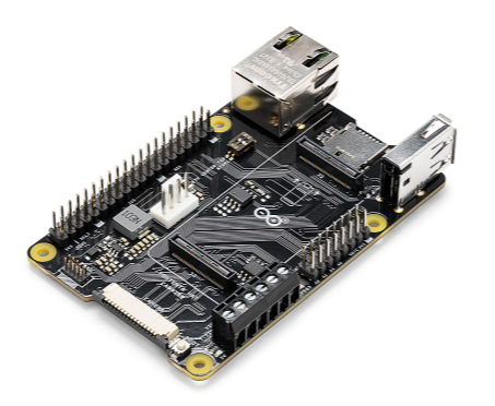
ASX00049

Arduino

* $43.78 - * $50.68

IN STOCK 2855
Buy

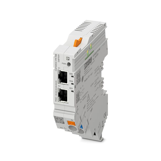
1687559

Phoenix Contact Ltd

[no prices available]

IN STOCK 2
Buy

Reference Designs

RD006

Wurth Elektronik

RD006 - 3 W Dual-output isolated auxiliary supply for communication interfaces and measurement systems

CN0583

Analog Devices Inc.

Multistandard Micropower Verified Smoke Detection System-on-Module

Technical Resources

EVALUATION KITS

EVAL-AD7124-8SDZ

Analog Devices Inc.

$0.00 - * $82.19

IN STOCK 792
Buy
View All