
LTC3867EUF Demo Board | 4.5 ≤ VIN ≤ 14V, VOUT = 1.5V @ 15A
Analog Devices Inc.Demonstration circuit 1771A is a single output synchronous buck converter featuring the LTC3867EUF with a 24-lead 4mm × 4mm QFN package. The input voltage range is from 4.5V to 14V and it provides 1.5V at 15A at the output. The DC1771A is configured with a sense resistor.
DCR sensing circuit is optional. Using the inductor’s DCR as the sense element instead of the on-board sense resistor saves cost and board space while improving full-load efficiency over 2%, though the sense resistor provides a more accurate current limit.

LTC6430-15 100-400MHz board
Analog Devices Inc.DC1774A-A: Demo Board for the LTC6430-15 High Linearity Differential RF/IF Amplifier/ADC Driver.

LTC2378-18 with LTC6655-5/LT6350 Demo Board | 18-Bit, 1Msps, SAR ADC with 102dB SNR. Requires DC718 or DC2026
Analog Devices Inc.The LTC2380/LTC2379/LTC2378/LTC2377/LTC2376 are low power, low noise ADCs with serial outputs that can operate from a single 2.5V supply. The demo manual refers to the LTC2379-18 but applies to all parts in the family, the only difference being the maximum sample rates and the number of bits. The LTC2379-18 supports a ±5V fully differential input range with a 101dB SNR, consumes only 18mW and achieves ±2LSB INL max with no missing codes at 18-bits. The DC1783A demonstrates the DC and AC performance of the LTC2379-18 in conjunction with the DC590 QuikEval™ and DC718 PScope™ data collection boards.

LTC1418CG | Low Power 14-Bit ADC Serial/Parallel Interface
Analog Devices Inc.DC178A: Demo Board for the LTC1418 Low Power, 14-Bit, 200ksps ADC with Serial and Parallel I/O.

DC1791A-B
Analog Devices Inc.The LTM2887 is a complete galvanic digital ?Module? (micromodule) isolator. No external components are required. A single 3.3V or 5V supply powers both sides of the interface through an integrated, isolated DC/DC converter. A logic supply pin allows easy interfacing with different logic levels from 1.62V to 5.5V, independent of the main supply.Available options are compliant with SPI and I2C (master mode only) specifications.The isolated side includes two 5V nominal power supplies, including programmable current limit, each capable of providing more than 100mA of load current. The supplies may be adjusted from their nominal value using a single external resistor.Coupled inductors and an isolation power transformer provide 2500VRMS of isolation between the input and output logic interface. This device is ideal for systems where the ground loop is broken, allowing for a large common mode voltage range. Communication is uninterrupted for common mode transients greater than 30kV/?s.Applications Isolated SPI or I2C Interfaces Industrial Systems Test and Measurement Equipment Breaking Ground Loops

DC1794A
Analog Devices Inc.The LTM2885 is a complete galvanically isolated full-duplex RS485/RS422 ?Module? (micromodule) transceiver. No external components are required. A single supply powers both sides of the interface through an integrated, isolated, low noise, efficient 5V output DC/DC converter.Coupled inductors and an isolation power transformer provide 6500VRMS of isolation between the line transceiver and the logic interface. This device is ideal for systems where the ground loop is broken allowing for large common mode voltage variation. Uninterrupted communication is guaranteed for common mode transients up to 50kV/?s.Maximum data rates are 20Mbps or 250kbps in slew limited mode. Transmit data, DI, and receive data, RO, are implemented with event driven low jitter processing. The receiver has a one-eighth unit load supporting up to 256 nodes per bus. A logic supply pin allows easy interfacing with different logic levels from 1.62V to 5.5V, independent of the main supply.Enhanced ESD protection allows this part to withstand up to ?15kV (human body model) on the transceiver interface pins to isolated supplies and ?25kV through the isolation barrier to logic supplies without latch-up or damage.APPLICATIONS Isolated RS485/RS422 Interface Industrial Networks Breaking RS485 Ground Loops Isolated PROFIBUS-DP Networks

LTC6360 Driving LTC2367-18 Demo Board | 18-Bit, 0.5Msps SAR ADC (Requires DC590 or DC718)
Analog Devices Inc.DC1796A-G Demo Board for:
LTC6360 Very Low Noise Single-Ended SAR ADC Driver with True Zero Output
LTC2367-18 18-Bit, 500ksps, Pseudo-Differential Unipolar SAR ADC with 97dB SNR

DC1801A-A
Analog Devices Inc.The LTC3838 is a dual, PolyPhase? synchronous step-down DC/DC switching regulator controller. Two independent channels drive all N-channel power MOSFETs. The controlled on-time, valley current mode control architecture allows for fast transient response and constant frequency switching in steady-state operation, independent of VIN, VOUT and load current. Its load-release transient detection feature significantly reduces overshoot at low output voltages.Differential output voltage sensing, along with a precision internal reference, offers an accurate ?0.67% output regulation on Channel 1, even if the remote output ground deviates from local ground by ?500mV. The second channel can either provide an independent ?1% output, or together with the first channel of this controller, serve as one of the PolyPhase channels for a single-output voltage.The switching frequency can be programmed from 200kHz to 2MHz with an external resistor, and can be synchronized to an external clock. Very low tON and tOFF times allow for near 0% and near 100% duty cycles, respectively. Voltage tracking soft start-up and multiple safety features are provided.See below for a comparison of LTC3838, LTC3838-1 and LTC3838-2. Part Number Description LTC3838 ? ?0.67% Differential Output Voltage Accuracy Over Temperature on Channel 1, ?1% Output Regulation on Channel 2, Separate Per Channel 30mV to 100mV Current Sense Range Controls LTC3838-1 ? ?0.67% Differential Output Voltage Accuracy Over Temperature on Both Channel 1 and Channel 2, Single Pin 30mV/60mV Current Sense Range Controls LTC3838-2 ?0.67% Differential Output Voltage Accuracy With Internal Reference on Channel 1, ?4mV Differential with External Reference Voltage on Channel 2, Fixed 30mV Current Sense Range Applications Distributed Power Systems Point-of-Load Converters Computing Systems Data Communication Systems

LTC3245EMSE Demo Board | Buck-Boost Charge Pump, 2.7V ≤ VIN ≤ 38V, VOUT = 1.2V/3.3V/5V @ 250mA
Analog Devices Inc.Demonstration circuit DC1802A is a wide VIN range, low noise, 250mA buck-boost charge pump featuring the LTC3245EMSE. It has an input supply range of 2.7V to 38V and provides a jumper-selectable 5V, 3.3V, or adjustable output (set to 1.2V) at 250mA.
LTC6362 with 1Msps 18-bit LTC2378-18 Demo Board | SAR ADC, LTC6655-5. Requires DC718 or DC2026
Analog Devices Inc.The LTC6362 is a low power, low noise differential op amp with rail-to-rail input and output swing that has been optimized to drive low power SAR ADCs. The amplifier may be configured to buffer a fully differential input signal or convert a single-ended input signal to a differential output signal.
DC1813A-B
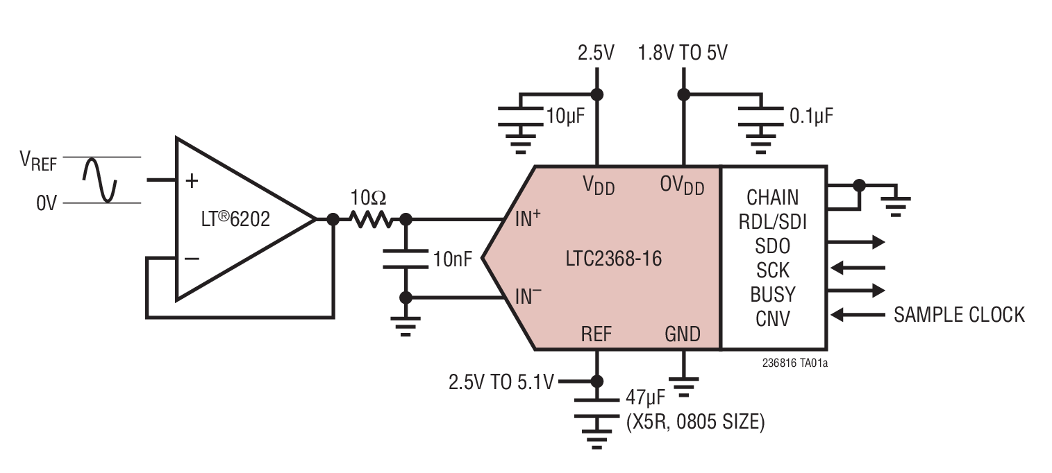
Analog Devices Inc.The LTC2368-16 is a low noise, low power, high speed 16-bit successive approximation register (SAR) ADC. Operating from a 2.5V supply, the LTC2368-16 has a 0V to VREF pseudo-differential unipolar input range with VREF ranging from 2.5V to 5.1V. The LTC2368-16 consumes only 13.5mW and achieves ?0.75LSB INL maximum, no missing codes at 16 bits with 94.7dB SNR.The LTC2368-16 has a high speed SPI-compatible serial interface that supports 1.8V, 2.5V, 3.3V and 5V logic while also featuring a daisy-chain mode. The fast 2Msps throughput with no cycle latency makes the LTC2368-16 ideally suited for a wide variety of high speed applications. An internal oscillator sets the conversion time, easing external timing considerations. The LTC2368-16 automatically powers down between conversions, leading to reduced power dissipation that scales with the sampling rate.Applications Medical Imaging High Speed Data Acquisition Portable or Compact Instrumentation Industrial Process Control Low Power Battery-Operated Instrumentation ATE

LTC2367-16 with LTC6655-5/LT6202 Demo Board |16-Bit, 500ksps, Pseudo-Differential Unipolar SAR ADC with 94.7dB SNR. Requires DC718 or DC590
Analog Devices Inc.DC1813A-C Demo Board for:
LTC2367-16 16-Bit, 500ksps, Pseudo- Differential Unipolar SAR ADC with 94.7dB SNR
LT6202 Single 100MHz, Rail-to-Rail Input and Output, Ultralow 1.9nVrtHz Noise, Low Power Op Amps
LTC6655 0.25ppm Noise, Low Drift Precision References

DC1813A-E
Analog Devices Inc.The LTC2369-18 is a low noise, low power, high speed 18-bit successive approximation register (SAR) ADC. Operating from a 2.5V supply, the LTC2369-18 has a 0V to VREF pseudo-differential unipolar input range with VREF ranging from 2.5V to 5.1V. The LTC2369-18 consumes only 18mW and achieves ?2.5LSB INL maximum, no missing codes at 18 bits with 96.5dB SNR.The LTC2369-18 has a high speed SPI-compatible serial interface that supports 1.8V, 2.5V, 3.3V and 5V logic while also featuring a daisy-chain mode. The fast 1.6Msps throughput with no cycle latency makes the LTC2369-18 ideally suited for a wide variety of high speed applications. An internal oscillator sets the conversion time, easing external timing considerations. The LTC2369-18 automatically powers down between conversions, leading to reduced power dissipation that scales with the sampling rate.Applications Medical Imaging High Speed Data Acquisition Portable or Compact Instrumentation Industrial Process Control Low Power Battery-Operated Instrumentation ATE

DC1816B
Analog Devices Inc.The LT3799-1 is an isolated flyback controller with power factor correction specifically designed for driving LEDs. The controller operates using critical conduction mode allowing the use of a small transformer. Using a novel current sensing scheme, the controller is able to deliver a well regulated current to the secondary side without using an opto-coupler. A strong gate driver is included to drive an external high voltage MOSFET. Utilizing an onboard multiplier, the LT3799-1 typically achieves power factors of 0.97. The FAULT pin provides notification of open and short LED conditions. The LT3799-1 offers improved line regulation over the LT3799, but is not designed for use with a TRIAC dimmer.The LT3799-1 uses a micropower hysteretic start-up to efficiently operate at offline input voltages, with a third winding to provide power to the part. An internal LDO provides a well regulated supply for the part?s internal circuitry and gate driver. Triac Dimmable LED Current Regulator LT3799 Yes ? 10% LT3799-1 No ? 5% Applications Offline 4W to 100W+ LED Applications High DC VIN LED Applications

LTM8001EY Demo Board | 5A Buck µModule Regulator, 6V ≤ VIN ≤ 36V, VOUT = Up to 5-Output Configurable LDO Array
Analog Devices Inc.Demo circuit 1818A features the LTM8001 μModule regulator that includes a 5A switching regulator and an array of five 1.1A low noise LDOs. The demo board operates from a 6V to 36V input and is configured so the switching regulator provides an output that also powers the LDOs. The LDOs in turn provide three outputs – one from a single LDO and two outputs each formed by paralleling two LDOs together.

LTC2389-18 with LTC6655/LT6201, 18-Bit, 2.5Msps, Serial/Parallel SAR ADC with 99.8dB SNR. Requires DC718
Analog Devices Inc.DC1826A-A Demo Board for:
LTC2389-18 18-Bit, 2.5Msps SAR ADC with Pin-Configurable Analog Input Range and 99.8dB SNR
LTC6655 0.25ppm Noise, Low Drift Precision References
LT6201 Dual 165MHz, Rail-to-Rail Input and Output, 0.95nV/√Hz Low Noise, Op Amp Family

DC1827A
Analog Devices Inc.The LT3795 is a DC/DC controller designed to regulate a constant-current or constant-voltage and is ideal for driving LEDs. It drives a low side external N-channel power MOSFET from an internal regulated 7.7V supply. The fixed frequency and current mode architecture result in stable operation over a wide range of supply and output voltages. Spread spectrum frequency modulation (SSFM) can be activated for improved electromagnetic compatibility (EMC) performance. The ground referred voltage FB pin serves as the input for several LED protection features, and also allows the converter to operate as a constant-voltage source. The maximum output current is set by an external resistor, and the output current amplifier has a rail-to-rail common mode range. The LT3795 also includes a separate input current sensing amplifier that is used to limit input current. The TG pin inverts and level shifts the PWM signal to drive the gate of the external PMOS. The PWM input provides LED dimming ratios of up to 3000:1, and the CTRL inputs provide additional analog dimming capability.APPLICATIONS High Power LED, High Voltage LED Battery Chargers Accurate Current Limited Voltage Regulators

DC182A
Analog Devices Inc.The LT1786F is a fixed frequency, current mode, switching regulator that provides the control function for Cold Cathode Fluorescent Lighting (CCFL). The IC includes an efficient high current switch, an oscillator, output drive logic, control circuitry and a micropower 6-bit 100?A full-scale current output DAC. The DAC provides simple ?bits-to-lamp-current control? and communicates using the 2-wire SMBus serial interface. The LT1786F acts as an SMBus slave device using one of two selectable SMBus addresses set by the address pin ADR.On Power-up, the DAC output current assumes midrange or zero scale, depending on the logic state of the ADR pin.The entire IC can be shut down through the SMBSUS pin or by setting the SHDN bit = 1 in the SMBus command byte. Digital data for the DAC output current is retained internally and the supply current drops to 40?A for standby operation. The active low SHDN pin disables the CCFL control circuitry, but keeps the DAC alive. Supply current in this operating mode drops to 150?A.The LT1786F control circuitry operates from a logic supply voltage of 3.3V or 5V. The IC also has a battery supply pin that operates from 4.5V to 30V. The LT1786F draws 6mA typical quiescent current. A 200kHz switching frequency minimizes magnetic component size. Current mode switching techniques with cycle-by-cycle limiting gives high reliability and simple loop frequency compensation. The LT1786F is available in a 16-pin narrow SO package.Applications Notebook and Palmtop Computers Portable Instruments Personal Digital Assistants

LTC4000EGN Battery Charger Controller and PowerPath Manager
Analog Devices Inc.Demonstration circuit 1830B is a battery charger controller and PowerPath™ manager featuring the LTC4000. This board should be connected to a front end DC/DC power supply for a complete charger solution.

LTC4000-1 Battery Charger Controller and PowerPath Manager with Maximum Power Point Control
Analog Devices Inc.Demonstration circuit 1830B is a battery charger controller and PowerPath™ manager with maximum power point control (MPPC) featuring the LTC4000-1. MPPC extracts near maximum power from high impedance sources such as solar panels, wind turbines or fuel cells. MPPC is achieved by means of an input voltage regulation control loop. This board should be connected to a front-end DC/DC power supply for a complete charger solution.


